P14nf12fp - 120v, 14a 3e1f1t
This document was ed by and they confirmed that they have the permission to share it. If you are author or own the copyright of this book, please report to us by using this report form. Report r6l17
Overview 4q3b3c
& View P14nf12fp - 120v, 14a as PDF for free.
More details 26j3b
- Words: 1,147
- Pages: 9
STP14NF12 STP14NF12FP N-CHANNEL 120V - 0.16Ω - 14A TO-220/TO-220FP LOW GATE CHARGE STripFET™ POWER MOSFET TYPE STP14NF12 STP14NF12FP ■ ■ ■
VDSS
RDS(on)
ID
120 V 120 V
< 0.18 Ω < 0.18 Ω
14 A 14 A
TYPICAL RDS(on) = 0.16Ω EXCEPTIONAL dv/dt CAPABILITY APPLICATION ORIENTED CHARACTERIZATION
3
3 1
2
1
TO-220 DESCRIPTION This Power MOSFET series realized with STMicroelectronics unique STripFET process has specifically been designed to minimize input capacitance and gate charge. It is therefore suitable as primary switch in advanced high-efficiency isolated DC-DC converters for Telecom and Computer application. It is also intended for any application with low gate charge drive requirements
2
TO-220FP
INTERNAL SCHEMATIC DIAGRAM
APPLICATIONS HIGH-EFFICIENCY DC-DC CONVERTERS ■ UPS AND MOTOR CONTROL ■
ABSOLUTE MAXIMUM RATINGS Symbol
Parameter
Value STP14NF12
VDS VDGR VGS
120
V
Drain-gate Voltage (RGS = 20 kΩ)
120
V
Gate- source Voltage
±20
V
Drain Current (continuous) at TC = 25°C
ID
Drain Current (continuous) at TC = 100°C Drain Current (pulsed) Total Dissipation at TC = 25°C
60
Derating Factor
0.4
PTOT
STP14NF12FP
Drain-source Voltage (VGS = 0)
ID IDM ()
Unit
14
8.5
A
9
6
A
56
34
A
25
W
0.17
W/°C
dv/dt (1)
Peak Diode Recovery voltage slope
9
V/ns
EAS (2)
Single Pulse Avalanche Energy
60
mJ
VISO Tj Tstg
Insulation Withstand Voltage (DC) Operating Junction Temperature Storage Temperature
(● ) Pulse width limited by safe operating area
August 2002
-
2500 -55 to 175
V °C
(1) ISD ≤14A, di/dt ≤300A/µs, VDD ≤ V(BR)DSS, Tj ≤ T JMAX. (2) Starting Tj = 25°C, ID = 14A, VDD = 50V
1/9
STP14NF12/STP14NF12FP THERMAL DATA TO-220
TO-220FP
2.5
6
Rthj-case
Thermal Resistance Junction-case Max
Rthj-amb
Thermal Resistance Junction-ambient Max
62.5
°C/W
Maximum Lead Temperature For Soldering Purpose
300
°C
Tl
°C/W
ELECTRICAL CHARACTERISTICS (TCASE = 25 °C UNLESS OTHERWISE SPECIFIED) OFF Symbol
Parameter
Test Conditions
Drain-source Breakdown Voltage
ID = 250 µA, VGS = 0
IDSS
Zero Gate Voltage Drain Current (VGS = 0)
VDS = Max Rating
IGSS
Gate-body Leakage Current (VDS = 0)
VGS = ±20V
V(BR)DSS
Min.
Typ.
Max.
120
Unit V
VDS = Max Rating, TC = 125 °C
1
µA
10
µA
±100
nA
ON (1) Symbol
Parameter
Test Conditions
VGS(th)
Gate Threshold Voltage
VDS = VGS, ID = 250µA
RDS(on)
Static Drain-source On Resistance
VGS = 10V, ID = 7 A
Min.
Typ.
Max.
Unit
2
3
4
V
0.16
0.18
Ω
Typ.
Max.
Unit
DYNAMIC Symbol gfs (1)
2/9
Parameter Forward Transconductance
Test Conditions VDS = 15V , ID = 7 A VDS = 25V, f = 1 MHz, VGS = 0
Min.
4
S
460
pF
Ciss
Input Capacitance
Coss
Output Capacitance
70
pF
Crss
Reverse Transfer Capacitance
30
pF
STP14NF12/STP14NF12FP ELECTRICAL CHARACTERISTICS (CONTINUED) SWITCHING ON Symbol td(on) tr Qg Qgs Qgd
Parameter Turn-on Delay Time Rise Time Total Gate Charge Gate-Source Charge Gate-Drain Charge
Test Conditions
Min.
VDD = 50 V, ID = 7 A RG = 4.7Ω VGS = 10V (Resistive Load, see Figure 3) VDD = 80 V, ID = 14 A, VGS = 10V
Typ.
Max.
Unit
16
ns
25
ns
15.5 3.7 4.7
21
nC nC nC
Typ.
Max.
Unit
SWITCHING OFF Symbol td(off) tf
Parameter Turn-off-Delay Time Fall Time
Test Conditions
Min.
32 8
VDD = 50 V, ID = 7 A, RG = 4.7Ω, VGS = 10V (Resistive Load, see Figure 3)
ns ns
SOURCE DRAIN DIODE Symbol ISD
Parameter
Test Conditions
Source-drain Current (pulsed)
VSD (1)
Forward On Voltage
ISD = 14 A, VGS = 0
Reverse Recovery Time Reverse Recovery Charge Reverse Recovery Current
ISD = 14 A, di/dt = 100A/µs, VDD = 50 V, Tj = 150°C (see test circuit, Figure 5)
IRRM
Typ.
Source-drain Current
ISDM (2) trr Qrr
Min.
Max.
Unit
14
A
56
A
1.5
V
92 230 5
ns nC A
Note: 1. Pulsed: Pulse duration = 300 µs, duty cycle 1.5 %. 2. Pulse width limited by safe operating area.
Safe Operating Area For TO-220
Safe Operating Area For TO-220FP
3/9
STP14NF12/STP14NF12FP Thermal Impedance For TO-220
Thermal Impedance For TO-220FP
Output Characteristics
Transfer Characteristics
Transconductance
Static Drain-source On Resistance
4/9
STP14NF12/STP14NF12FP Gate Charge vs Gate-source Voltage
Capacitance Variations
Normalized Gate Threshold Voltage vs Temp.
Normalized On Resistance vs Temperature
Source-drain Diode Forward Characteristics
Normalized BVDSS vs Temperature
5/9
STP14NF12/STP14NF12FP Fig. 1: Unclamped Inductive Load Test Circuit
Fig. 2: Unclamped Inductive Waveform
Fig. 3: Switching Times Test Circuit For Resistive Load
Fig. 4: Gate Charge test Circuit
Fig. 5: Test Circuit For Inductive Load Switching And Diode Recovery Times
6/9
STP14NF12/STP14NF12FP
TO-220 MECHANICAL DATA DIM.
mm. MIN.
TYP
inch MAX.
MIN.
TYP.
MAX.
A
4.40
4.60
0.173
0.181
C
1.23
1.32
0.048
0.051
D
2.40
2.72
0.094
0.107
E
0.49
0.70
0.019
0.027
F
0.61
0.88
0.024
0.034
F1
1.14
1.70
0.044
0.066
F2
1.14
1.70
0.044
0.066
G
4.95
5.15
0.194
0.202
G1
2.40
2.70
0.094
0.106
H2
10
10.40
0.393
0.409
L2
16.40
L3
28.90
L4
13
0.645 1.137 14
0.511
0.551
L5
2.65
2.95
0.104
0.116
L6
15.25
15.75
0.600
0.620
L7
6.20
6.60
0.244
0.259
L9
3.50
3.93
0.137
0.154
DIA
3.75
3.85
0.147
0.151
1
7/9
STP14NF12/STP14NF12FP
TO-220FP MECHANICAL DATA mm.
DIM.
MIN.
inch
TYP
MAX.
MIN.
TYP.
MAX.
A
4.4
4.6
0.173
0.181
B
2.5
2.7
0.098
0.106
D
2.5
2.75
0.098
0.108
E
0.45
0.7
0.017
0.027
F
0.75
1
0.030
0.039
F1
1.15
1.7
0.045
0.067
F2
1.15
1.7
0.045
0.067
G
4.95
5.2
0.195
0.204
G1
2.4
2.7
0.094
0.106
H
10
10.4
0.393
0.409
L2
16
0.630
L3
28.6
30.6
1.126
1.204
L4
9.8
10.6
.0385
0.417
L5
2.9
3.6
0.114
0.141
L6
15.9
16.4
0.626
0.645
9
9.3
0.354
0.366
Ø
3
3.2
0.118
0.126
B
D
A
E
L7
L3 L6
F2
H
G
G1
F
F1
L7
L2
8/9
L5
1 2 3 L4
STP14NF12/STP14NF12FP
Information furnished is believed to be accurate and reliable. However, STMicroelectronics assumes no responsibility for the consequences of use of such information nor for any infringement of patents or other rights of third parties which may result from its use. No license is granted by implication or otherwise under any patent or patent rights of STMicroelectronics. Specifications mentioned in this publication are subject to change without notice. This publication supersedes and replaces all information previously supplied. STMicroelectronics products are not authorized for use as critical components in life devices or systems without express written approval of STMicroelectronics. © The ST logo is a ed trademark of STMicroelectronics © 2002 STMicroelectronics - Printed in Italy - All Rights Reserved STMicroelectronics GROUP OF COMPANIES Australia - Brazil - Canada - China - Finland - - - Hong Kong - India - Israel - Italy - Japan - Malaysia - Malta - Morocco Singapore - Spain - Sweden - Switzerland - United Kingdom - United States. © http://www.st.com
9/9
Related Documents 171j1w

P14nf12fp - 120v, 14a 3e1f1t
March 2021 0
Dl-14a 2w4g4w
November 2019 47
Borang 14a 331v43
November 2022 0
Api 14a 4o294o
November 2019 26
14a. Formulir Cuti Pasien.doc 7606q
April 2020 12
Fbt Promaxx 14a Pdf 474e3n
October 2019 24More Documents from "RenatoMaia" 275d1s
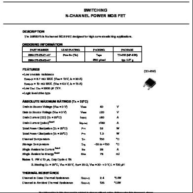
2sk4075 - 40v,60a 1y4t1o
August 2021 0
Jax-pk8 425f2k
July 2022 0
2c82t
March 2021 0
P14nf12fp - 120v, 14a 3e1f1t
March 2021 0
Vpl-es5_ex5_ex50_ex5u_ew5_ 71g3n
September 2022 0