Timing Diagram - 8085.pdf 6t2z2c
This document was ed by and they confirmed that they have the permission to share it. If you are author or own the copyright of this book, please report to us by using this report form. Report r6l17
Overview 4q3b3c
& View Timing Diagram - 8085.pdf as PDF for free.
More details 26j3b
- Words: 1,055
- Pages: 5
6/26/2016
Timing Diagram 8085 Microprocessor Course
Home
Laboratories
Quizzes
Sitemap
Us
You Are Here : Home » Embedded Lab » 8085 Microprocessor » Timing Diagrams
Articles added in Mathematics Lab | Cyber Lab is now open | Astronomy Lab is now open | VLSI Lab is now o
Timing Diagrams of 8085 It is one of the best way to understand to process of microprocessor/controller. With the help of timing diagram we can understand the working of any system, step by step working of each instruction and its execution, etc. It is the graphical representation of process in steps with respect to time. The timing diagram represents the clock cycle and duration, delay, content of address bus and data bus, type of operation ie. Read/write/status signals.
Important related to timing diagrams: 1. Instruction cycle: this term is defined as the number of steps required by the u to complete the entire process ie. Fetching and execution of one instruction. The fetch and execute cycles are carried out in synchronization with the clock. 2. Machine cycle: It is the time required by the microprocessor to complete the operation of accessing the memory devices or I/O devices. In machine cycle various operations like opcode fetch, memory read, memory write, I/O read, I/O write are performed. 3. Tstate: Each clock cycle is called as Tstates.
Rules to identify number of machine cycles in an instruction: 1. If an addressing mode is direct, immediate or implicit then No. of machine cycles = No. of bytes. 2. If the addressing mode is indirect then No. of machine cycles = No. of bytes + 1. Add +1 to the No. of machine cycles if it is memory read/write operation. 3. If the operand is 8bit or 16bit address then, No. of machine cycles = No. of bytes +1. 4. These rules are applicable to 80% of the instructions of 8085. Timing Diagram:
Where, Instruction cycle= Fetch Cycle(FC) + Executecycle(EC).
Tweets by @z_series
Opcode fetch: The microprocessor requires instructions to perform any particular action. In order to perform these actions microprocessor utilizes Opcode which is a part of an instruction which provides detail(ie. Which operation µp needs to perform) to microprocessor.
http://www.zseries.in/embedded%20lab/8085%20microprocessor/timing%20diagram.php
1/5
6/26/2016
Timing Diagram 8085 Microprocessor Course
Fig: Opcode fetch timing diagram Operation: During T1 state, microprocessor uses IO/M(bar), S0, S1 signals are used to instruct microprocessor to fetch opcode. Thus when IO/M(bar)=0, S0=S1= 1, it indicates opcode fetch operation. During this operation 8085 transmits 16bit address and also uses ALE signal for address latching. At T2 state microprocessor uses read signal and make data ready from that memory location to read opcode from memory and at the same time program counter increments by 1 and points next instruction to be fetched. In this state microprocessor also checks READY input signal, if this pin is at low logic level ie. '0' then microprocessor adds wait state immediately between T2 and T3. At T3, microprocessor reads opcode and store it into instruction to decode it further. During T4 microprocessor performs internal operation like decoding opcode and providing necessary actions. The opcode is decoded to know whether T5 or T6 states are required, if they are not required then µp performs next operation.
Read and write timing diagram for memory and I/O Operation
Memory Read:
<>Figure: Memory read timing diagram
http://www.zseries.in/embedded%20lab/8085%20microprocessor/timing%20diagram.php
2/5
6/26/2016
Timing Diagram 8085 Microprocessor Course Operation: It is used to fetch one byte from the memory. It requires 3 TStates. It can be used to fetch operand or data from the memory.
During T1, A8A15 contains higher byte of address. At the same time ALE is high. Therefore Lower byte of address A0A7 is selected from AD0AD7. Since it is memory ready operation, IO/M(bar) goes low. During T2 ALE goes low, RD(bar) goes low. Address is removed from AD0AD7 and data D0D7 appears on AD0AD7. During T3, Data remains on AD0AD7 till RD(bar) is at low signal.
Memory Write:
Figure: Memory write timing diagram Operation: It is used to send one byte into memory. It requires 3 TStates. During T1, ALE is high and contains lower address A0A7 from AD0AD7. A8A15 contains higher byte of address. As it is memory operation, IO/M(bar) goes low. During T2, ALE goes low, WR(bar) goes low and Address is removed from AD0AD7 and then data appears on AD0AD7. Data remains on AD0AD7 till WR(bar) is low.
IO Read:
http://www.zseries.in/embedded%20lab/8085%20microprocessor/timing%20diagram.php
3/5
6/26/2016
Timing Diagram 8085 Microprocessor Course
Figure: I/O read timing diagram Operation: It is used to fetch one byte from an IO port. It requires 3 TStates. During T1, The Lower Byte of IO address is duplicated into higher order address bus A8A15. ALE is high and AD0AD7 contains address of IO device. IO/M (bar) goes high as it is an IO operation. During T2, ALE goes low, RD (bar) goes low and data appears on AD0AD7 as input from IO device. During T3 Data remains on AD0AD7 till RD(bar) is low.
IO Write:
Figure:I/O write timing diagram Operation: It is used to writ one byte into IO device. It requires 3 TStates.
http://www.zseries.in/embedded%20lab/8085%20microprocessor/timing%20diagram.php
4/5
6/26/2016
Timing Diagram 8085 Microprocessor Course During T1, the lower byte of address is duplicated into higher order address bus A8A15. ALE is high and A0A7 address is selected from AD0AD7. As it is an IO operation IO/M (bar) goes low.
During T2, ALE goes low, WR (bar) goes low and data appears on AD0AD7 to write data into IO device. During T3, Data remains on AD0AD7 till WR(bar) is low.
Comments sign in
Leave your comment...
Newest
Share Subscribe
RSS
Be the first to comment.
CACKLE comment system
About Us! 'Z Series Innovations' is an elearning solution for learning all technical stuff
Our Works! Z Series Innovations Trailer [Of䐆怀...
online. It is an online portal that gives an
Us Do you feel like contributing to this website technically? Jump in! Your technical expertise would be needed to create quality articles and content on this site and hence contribute to this growing global community of technical enthusiast.
enhanced way of learning and guidance in various fields of engineering which include robotics, electronics, communication,computer science, embedded systems and its real life applications.
Create quality content and get recognized!
Z Series Innovations © 20112015
http://www.zseries.in/embedded%20lab/8085%20microprocessor/timing%20diagram.php
5/5
Timing Diagram 8085 Microprocessor Course
Home
Laboratories
Quizzes
Sitemap
Us
You Are Here : Home » Embedded Lab » 8085 Microprocessor » Timing Diagrams
Articles added in Mathematics Lab | Cyber Lab is now open | Astronomy Lab is now open | VLSI Lab is now o
Timing Diagrams of 8085 It is one of the best way to understand to process of microprocessor/controller. With the help of timing diagram we can understand the working of any system, step by step working of each instruction and its execution, etc. It is the graphical representation of process in steps with respect to time. The timing diagram represents the clock cycle and duration, delay, content of address bus and data bus, type of operation ie. Read/write/status signals.
Important related to timing diagrams: 1. Instruction cycle: this term is defined as the number of steps required by the u to complete the entire process ie. Fetching and execution of one instruction. The fetch and execute cycles are carried out in synchronization with the clock. 2. Machine cycle: It is the time required by the microprocessor to complete the operation of accessing the memory devices or I/O devices. In machine cycle various operations like opcode fetch, memory read, memory write, I/O read, I/O write are performed. 3. Tstate: Each clock cycle is called as Tstates.
Rules to identify number of machine cycles in an instruction: 1. If an addressing mode is direct, immediate or implicit then No. of machine cycles = No. of bytes. 2. If the addressing mode is indirect then No. of machine cycles = No. of bytes + 1. Add +1 to the No. of machine cycles if it is memory read/write operation. 3. If the operand is 8bit or 16bit address then, No. of machine cycles = No. of bytes +1. 4. These rules are applicable to 80% of the instructions of 8085. Timing Diagram:
Where, Instruction cycle= Fetch Cycle(FC) + Executecycle(EC).
Tweets by @z_series
Opcode fetch: The microprocessor requires instructions to perform any particular action. In order to perform these actions microprocessor utilizes Opcode which is a part of an instruction which provides detail(ie. Which operation µp needs to perform) to microprocessor.
http://www.zseries.in/embedded%20lab/8085%20microprocessor/timing%20diagram.php
1/5
6/26/2016
Timing Diagram 8085 Microprocessor Course
Fig: Opcode fetch timing diagram Operation: During T1 state, microprocessor uses IO/M(bar), S0, S1 signals are used to instruct microprocessor to fetch opcode. Thus when IO/M(bar)=0, S0=S1= 1, it indicates opcode fetch operation. During this operation 8085 transmits 16bit address and also uses ALE signal for address latching. At T2 state microprocessor uses read signal and make data ready from that memory location to read opcode from memory and at the same time program counter increments by 1 and points next instruction to be fetched. In this state microprocessor also checks READY input signal, if this pin is at low logic level ie. '0' then microprocessor adds wait state immediately between T2 and T3. At T3, microprocessor reads opcode and store it into instruction to decode it further. During T4 microprocessor performs internal operation like decoding opcode and providing necessary actions. The opcode is decoded to know whether T5 or T6 states are required, if they are not required then µp performs next operation.
Read and write timing diagram for memory and I/O Operation
Memory Read:
<>Figure: Memory read timing diagram
http://www.zseries.in/embedded%20lab/8085%20microprocessor/timing%20diagram.php
2/5
6/26/2016
Timing Diagram 8085 Microprocessor Course Operation: It is used to fetch one byte from the memory. It requires 3 TStates. It can be used to fetch operand or data from the memory.
During T1, A8A15 contains higher byte of address. At the same time ALE is high. Therefore Lower byte of address A0A7 is selected from AD0AD7. Since it is memory ready operation, IO/M(bar) goes low. During T2 ALE goes low, RD(bar) goes low. Address is removed from AD0AD7 and data D0D7 appears on AD0AD7. During T3, Data remains on AD0AD7 till RD(bar) is at low signal.
Memory Write:
Figure: Memory write timing diagram Operation: It is used to send one byte into memory. It requires 3 TStates. During T1, ALE is high and contains lower address A0A7 from AD0AD7. A8A15 contains higher byte of address. As it is memory operation, IO/M(bar) goes low. During T2, ALE goes low, WR(bar) goes low and Address is removed from AD0AD7 and then data appears on AD0AD7. Data remains on AD0AD7 till WR(bar) is low.
IO Read:
http://www.zseries.in/embedded%20lab/8085%20microprocessor/timing%20diagram.php
3/5
6/26/2016
Timing Diagram 8085 Microprocessor Course
Figure: I/O read timing diagram Operation: It is used to fetch one byte from an IO port. It requires 3 TStates. During T1, The Lower Byte of IO address is duplicated into higher order address bus A8A15. ALE is high and AD0AD7 contains address of IO device. IO/M (bar) goes high as it is an IO operation. During T2, ALE goes low, RD (bar) goes low and data appears on AD0AD7 as input from IO device. During T3 Data remains on AD0AD7 till RD(bar) is low.
IO Write:
Figure:I/O write timing diagram Operation: It is used to writ one byte into IO device. It requires 3 TStates.
http://www.zseries.in/embedded%20lab/8085%20microprocessor/timing%20diagram.php
4/5
6/26/2016
Timing Diagram 8085 Microprocessor Course During T1, the lower byte of address is duplicated into higher order address bus A8A15. ALE is high and A0A7 address is selected from AD0AD7. As it is an IO operation IO/M (bar) goes low.
During T2, ALE goes low, WR (bar) goes low and data appears on AD0AD7 to write data into IO device. During T3, Data remains on AD0AD7 till WR(bar) is low.
Comments sign in
Leave your comment...
Newest
Share Subscribe
RSS
Be the first to comment.
CACKLE comment system
About Us! 'Z Series Innovations' is an elearning solution for learning all technical stuff
Our Works! Z Series Innovations Trailer [Of䐆怀...
online. It is an online portal that gives an
Us Do you feel like contributing to this website technically? Jump in! Your technical expertise would be needed to create quality articles and content on this site and hence contribute to this growing global community of technical enthusiast.
enhanced way of learning and guidance in various fields of engineering which include robotics, electronics, communication,computer science, embedded systems and its real life applications.
Create quality content and get recognized!
Z Series Innovations © 20112015
http://www.zseries.in/embedded%20lab/8085%20microprocessor/timing%20diagram.php
5/5
Related Documents 171j1w
Timing Diagram Of 8085 2k1iy
November 2021 0
Timing Diagram - 8085.pdf 6t2z2c
October 2021 0
Ddr3 Timing Diagram 5t3f21
November 2019 28
Valve+timing+diagram 362o38
December 2019 40
Valve Timing Diagram b3f36
December 2019 40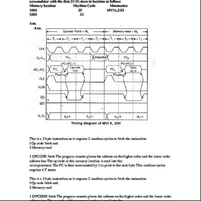
Timing Diagram Mvi A,32 4m2o3e
December 2019 36More Documents from "Amar" 504w24
Jessica Gomes Biography 50601i
December 2019 91
Beipackzettel Aspirin 500 Mg 8 St 10203595 Bz 476p6w
November 2019 100
Bc-details-sept17-07122017 (1) 376368
March 2023 0
Industry Analysis Project (indigo) 30s5h
October 2019 64
Timing Diagram - 8085.pdf 6t2z2c
October 2021 0