Photo Transistor 2u3g6r
This document was ed by and they confirmed that they have the permission to share it. If you are author or own the copyright of this book, please report to us by using this report form. Report r6l17
Overview 4q3b3c
& View Photo Transistor as PDF for free.
More details 26j3b
- Words: 1,953
- Pages: 8
18
Lab Experiments
Experiment-45
A
PHOTO TRANSISTOR CHARACTERISTICS Dr. Gabriel M. Rebeiz EECS Department, 1301 Beal Ave, The University of Michigan, Ann Arbor, MI 48109-2122. Email [email protected]
Abstract In a silicon phototransistor GT116 VCE versus IC, light intensity φ versus IC variations are studied using red, green, blue and white LED lights
Introduction A phototransistor is a silicon semiconductor device with photosensitive base. It consists of photodiode followed by a transistor as shown in Figutre-1. The photodiode supplies base current to the transistor, and the transistor multiplies the base current by its gain. The device responds to wide range of wavelength [1] varying from infrared to ultra violet. Phototransistor also responds to fluorescent and incandescent lights. However, phototransistors respond better to LED light. Hence LED light is used in this experiment. The output collector current is given by IC = hFE IP
…1
Where IC is collector current hFE is the current gain IP is photo current. Light Energy C E B
n C
n
o
p
o
C
o
B
E
E
B
Schmatic Symbol
TO-18 Package Bottom View
Figure-1, Phototransistor structure, base diagram and schematic symbol The current gain hFE is not a constant as in the case of bipolar junction transistor (BJT). It varies with light energy linearly up to a saturation point and there after decreases linearly. The variation
Vol-3, No-1, March - 2003
Lab Experiments
19
has a peak at certain input energy or wavelength. The VCE versus IC curve is similar to BJT with base current replaced by light energy. However, the curve is steeper with large output resistance.
Collector emitter saturation voltage -VCE (sat) In phototransistor, saturation condition is similar BJT, where both the collector base and base emitter junctions are forward biased. When saturated, the collector emitter voltage VCE(sat) decides how far the phototransistor approximate to a closed switch. These saturation voltages vary from 0.25V to 0.55V. Or when the collector emitter voltage is 0.25
<0.55V phototransistor is saturated.
Dark Current –ID When a phototransistor is placed in dark and voltage is applied across the collector emitter terminal a small current of the order of few nano ampere flows. This current is called dark current. This dark current is determined at VCE 5 to 20 volts. ID is of the order of 10 to 100nA and it is due to the minority carriers.
Breakdown Voltage V BR(CEO) The phototransistor should not be operated above certain voltage. The maximum allowable collector emitter voltage with base open is designated as Breakdown Voltage V BR(CEO). The value varies from 20 to 50 volts.
Acceptance angle This is a optical parameter speaks of focusing of light beam on to the photosensitive base area. It is the solid angle made by the light beam at the sensitive area. The double convex lens of the phototransistor converge the light beam to the sensitive area. Depending on the focal length of the lens used as light window this vary from 10-20 degree. Typical value for the GT116 transistor is 12 degree. Smaller the acceptance angle better is the focusing.
Capture area Surface area of the transparent window is called capture area. This area is about 12 mm2 for GT116 phototransistor. Light falling on this area only has an effect on the photo current.
LED light source LED light has been used in this experiment as source of light. The luminous intensity of this light along with material and peak wavelength is listed in Table-1 [2]. In this experiment, VCE versus IC curve is drawn for different color LED light energy. Variation of light intensity in Lux is studied with collector current at fixed VCE using blue and white light. Phototransistor is also operated with base connected to common, through a resistance RB [3]. Further, phototransistors can also be used as CE and CC amplifier similar to BJT.
Vol-3, No-1, March - 2003
20
Lab Experiments
Radiant Flux and Luminous Flux A point source of light emits light energy in all directions. The energy is transmitted in the form of photon. When photon falls on an eye the eye does not absorb all the photons. Eye selectively absorb these photons. The radiant flux φe is the average flow of radiant energy per unit time. It represents the total energy radiated by the source per unit time. The eye or an optical detector responds partially to the radiant energy. Hence the energy received by the eye is denoted as luminous flux φv. The radiant flux and luminous flux is connected by a equation given by φv = Kλφe
…2
Where φv is the luminous flux φe is the radiant flux Kλ luminous efficiency or the luminosity The subscripts ‘e’ refers to the radiation emitter and ‘v’ visibility by the observer. The radiant flux is denoted in watts. It is the product of current and voltage flowing in the radiation emitter. Luminous flux φv is represented in lumen. Hence the constant Kλ is lumen per watt. For semiconductor light sources such as LED, the luminosity [4] is calculated at various wavelengths and plotted in a graph shown in Figure-2. For the three different LEDs used in this experiment, knowing its wavelength [5,6] luminosity is evaluated from the curve in Figure-2 and presented in Table-1.
Luminosity (lumen/watt)
800 700 600 500 400 300 200 100 0 400
450
500
550
600
650
700
Wavelength (nm)
Figure-2, CIE*Spectral luminous efficiency curve for LED light source
Color Blue Red White
Table-1 Energy Radiant λ(nm) Kλ(Lumen/W) (eV) Flux φe (W) 469 2.50 0.090 90 627 1.87 0.050 180 540 2.17 0.090 500 Optical parameters of the LEDs used in this experiment
Vol-3, No-1, March - 2003
Luminosity φv (lumen) 8.1 9.0 40.0
Lab Experiments
21
Apparatus Used The experimental setup consists of a digital dc milliammeter 0-200mA; digital dc voltmeter 020V, dc regulated power supply 0-7volts and a LED light arrangement. The LED light arrangement is shown in Figure-3. It consists of connector rail with eight connecting pins. These pins are male connectors. The female is fixed to the LED module as shown in Figure-4. These modules are properly enclosed in a metallic enclosure and can be fitted to male socket at eight positions. By fixing the module at different positions on the rail, distance variation between the source and detector is achieved.
(a)
(b) Figure-3 (a) and (b), Led light arrangements
Figure-4, LED and phototransistor module
Vol-3, No-1, March - 2003
22
Lab Experiments
Experimental Procedure The experiment consists two parts Part A; Output characteristics of the phototransistor (VCE versus IC curve) Part-B; Variation of collector current with luminous intensity. Part A; Output characteristics of the phototransistor (VCE versus IC curve) 1. The circuit connections are made as shown in Figure-5. 10 Ohms IC
0-7Volts
VCE
C
V E
Figure-5, Circuit connections for phototransistor characteristics 2. In the light arrangement shown in figure-3(a), the collector is terminated in 2-mm red banana socket and emitter is terminated by green banana socket. 3. The power supply is adjusted to 0 volts. The blue color LED module is inserted in to the socket and blue light is allowed to fall on the phototransistor facing it on second connector as shown in Figure-3(b). 4. The distance between the LED light source and phototransistor is measured using vernier calipers. d = 3mm = 0.3cm =0.003m The voltage is set to 0.2 volts and corresponding current in the milliammeter is noted and recorded in Table-2 5. Voltage is varied in suitable steps up to a maximum of 7 volts and the corresponding collector current is noted in Table-2. 6. Experiment is repeated for white and red lights by replacing blue LED with white LED. The variation in the collector current is recorded in Table-2. 7. A graph is drawn taking collector emitter voltage VCE along X-axis and collector current along Y-axis as shown in Figure-4. 8. Experiment is repeated for white Led light and the corresponding collector current variations are noted for different collector-emitter voltage in Table-2.
Vol-3, No-1, March - 2003
23
Lab Experiments Table-2 Collector Current (mA) White Blue Red 0 0 0 0 0.2 5.2 9.8 2.1 0.4 8.2 14.4 3.5 0.6 9.1 15.3 4.1 0.8 10.0 16.5 4.5 1.0 11.0 17.3 4.7 1.5 12.8 19.1 4.9 2.0 14.6 21.1 4.9 3.0 17.4 24.5 5.1 4.0 19.7 27.3 5.2 5.0 21.1 29.8 5.3 6.0 22.0 32.0 5.3 7.0 22.8 33.7 5.4 Variation of collector current with different light energy VCE (V)
Collewctor Current (mA)
2.17KeV-White 40 35 30 25 20 15 10 5 0
2.5KeV-Blue"
1.87KeV-Red
5
0
2
4
6
8
Collector Emitter Voltage VCE (V)
Figure-4, Output characteristics of phototransistor Part-B; Variation of collector current with luminous intensity 9. The collector emitter voltage is set 5 volts. With blue LED light falling on the phototransistor at position-2 on the light arrangement, and the collector current is noted in Table –3. 10. Experiment is repeated by moving phototransistor in to 3,4 up 8 positions on the light arrangement. At each position VCE set to 5volts and collector current is noted. The distance between the light source and phototransistor is also noted. 11. Trial repeated for white lights. The corresponding photocurrent is noted in Table-3. Luminosity is determined taking lumen value of LED light using CIE curve shown in Figure2
Vol-3, No-1, March - 2003
24
Lab Experiments
12. A graph is drawn taking luminosity along X-axis and collector current along Y axis as shown in Figure-7. Table-3 Distance Blue White (m) IC (mA) IC (mA) φv (K Lux) φv (K Lux) 0.032 7.9 20.6 39.0 10.4 0.057 2.5 5.2 12.3 1.2 0.082 1.2 5.6 5.9 1.3 0.107 0.7 3.3 3.5 0.5 0.132 0.46 2.4 2.3 0.3 0.157 0.32 1.1 1.6 0.1 Collector current variation with light intensity
Position 3 4 5 6 7 8
25
Collector Current (mA)
Collector Current (mA)
Lumen 8.1 Luminous intensity = ---------- = ----------- = 7900 = 7.9K Lux d2 0.0322
20 15 10 5 0 0
2
4
6
8
10
12 10 8 6 4 2 0 0
Luminous Intensity (K Lux)
10
20
30
40
50
Luminous Intensity (K Lux)
(a) (b) Figure-7, Collector current variation with luminous intensity (a) with blue light (b) with white light
Results 1. The output characteristics curve of GT116 silicon phototransistor is similar to bipolar junction transistor with base current replaced by photon energy. 2. For the three LED lights blue, white and red the curves followed the same sequence 0f VIBGYOR of decreasing energy. 3. The output curves have steeper slope in comparison with BJT curves. This is because of the photodiode that actually detects the light inside the phototransistor. 4. The luminous intensity versus collector current curve is linear. This need not be the case for higher intensity [4].
Vol-3, No-1, March - 2003
Lab Experiments
25
Discussions A phototransistor characteristic is found similar to BJT characteristics with main difference in the output resistance (steep slope). The saturation voltage is also more than 0.3volts extends up to 0.55 volts. Phototransistors are made to use with Led light sources rather than incandescent (bulb) or fluorescent (tube) light. There are varieties of applications of phototransistors, which will be discussed, in future publications.
References [1]
Characteristics of phototransistor and photodarlingtons, EG&G Opto electronics, www.engr.udayton.edu/faculty/jloomis/ece445/topics/eggine/p_char.
[2]
M G Craford “LED challenge the incandescent” IEEE Circuits and Devices, Sept 1992.
[3]
Fairchild semiconductor Corporation, REV.4004/30/02, Application note AN3005, Design fundamentals for phototransistor circuits, www/fairchildsemi.com
[4]
Sharupich L, Tugov N, Optoelectronics, Page 17, 1987. Mir Publications.
[5]
Sharupich L, Tugov N, Optoelectronics, Page 85, 1987. Mir Publications.
[6]
Vaughan D Martin, Optoelectronics, Page-12
Note- CIE* - Commission Internationale de L’ Éclair, a French commission which has set this standard since more than 100 years.
Vol-3, No-1, March - 2003
Lab Experiments
Experiment-45
A
PHOTO TRANSISTOR CHARACTERISTICS Dr. Gabriel M. Rebeiz EECS Department, 1301 Beal Ave, The University of Michigan, Ann Arbor, MI 48109-2122. Email [email protected]
Abstract In a silicon phototransistor GT116 VCE versus IC, light intensity φ versus IC variations are studied using red, green, blue and white LED lights
Introduction A phototransistor is a silicon semiconductor device with photosensitive base. It consists of photodiode followed by a transistor as shown in Figutre-1. The photodiode supplies base current to the transistor, and the transistor multiplies the base current by its gain. The device responds to wide range of wavelength [1] varying from infrared to ultra violet. Phototransistor also responds to fluorescent and incandescent lights. However, phototransistors respond better to LED light. Hence LED light is used in this experiment. The output collector current is given by IC = hFE IP
…1
Where IC is collector current hFE is the current gain IP is photo current. Light Energy C E B
n C
n
o
p
o
C
o
B
E
E
B
Schmatic Symbol
TO-18 Package Bottom View
Figure-1, Phototransistor structure, base diagram and schematic symbol The current gain hFE is not a constant as in the case of bipolar junction transistor (BJT). It varies with light energy linearly up to a saturation point and there after decreases linearly. The variation
Vol-3, No-1, March - 2003
Lab Experiments
19
has a peak at certain input energy or wavelength. The VCE versus IC curve is similar to BJT with base current replaced by light energy. However, the curve is steeper with large output resistance.
Collector emitter saturation voltage -VCE (sat) In phototransistor, saturation condition is similar BJT, where both the collector base and base emitter junctions are forward biased. When saturated, the collector emitter voltage VCE(sat) decides how far the phototransistor approximate to a closed switch. These saturation voltages vary from 0.25V to 0.55V. Or when the collector emitter voltage is 0.25
Dark Current –ID When a phototransistor is placed in dark and voltage is applied across the collector emitter terminal a small current of the order of few nano ampere flows. This current is called dark current. This dark current is determined at VCE 5 to 20 volts. ID is of the order of 10 to 100nA and it is due to the minority carriers.
Breakdown Voltage V BR(CEO) The phototransistor should not be operated above certain voltage. The maximum allowable collector emitter voltage with base open is designated as Breakdown Voltage V BR(CEO). The value varies from 20 to 50 volts.
Acceptance angle This is a optical parameter speaks of focusing of light beam on to the photosensitive base area. It is the solid angle made by the light beam at the sensitive area. The double convex lens of the phototransistor converge the light beam to the sensitive area. Depending on the focal length of the lens used as light window this vary from 10-20 degree. Typical value for the GT116 transistor is 12 degree. Smaller the acceptance angle better is the focusing.
Capture area Surface area of the transparent window is called capture area. This area is about 12 mm2 for GT116 phototransistor. Light falling on this area only has an effect on the photo current.
LED light source LED light has been used in this experiment as source of light. The luminous intensity of this light along with material and peak wavelength is listed in Table-1 [2]. In this experiment, VCE versus IC curve is drawn for different color LED light energy. Variation of light intensity in Lux is studied with collector current at fixed VCE using blue and white light. Phototransistor is also operated with base connected to common, through a resistance RB [3]. Further, phototransistors can also be used as CE and CC amplifier similar to BJT.
Vol-3, No-1, March - 2003
20
Lab Experiments
Radiant Flux and Luminous Flux A point source of light emits light energy in all directions. The energy is transmitted in the form of photon. When photon falls on an eye the eye does not absorb all the photons. Eye selectively absorb these photons. The radiant flux φe is the average flow of radiant energy per unit time. It represents the total energy radiated by the source per unit time. The eye or an optical detector responds partially to the radiant energy. Hence the energy received by the eye is denoted as luminous flux φv. The radiant flux and luminous flux is connected by a equation given by φv = Kλφe
…2
Where φv is the luminous flux φe is the radiant flux Kλ luminous efficiency or the luminosity The subscripts ‘e’ refers to the radiation emitter and ‘v’ visibility by the observer. The radiant flux is denoted in watts. It is the product of current and voltage flowing in the radiation emitter. Luminous flux φv is represented in lumen. Hence the constant Kλ is lumen per watt. For semiconductor light sources such as LED, the luminosity [4] is calculated at various wavelengths and plotted in a graph shown in Figure-2. For the three different LEDs used in this experiment, knowing its wavelength [5,6] luminosity is evaluated from the curve in Figure-2 and presented in Table-1.
Luminosity (lumen/watt)
800 700 600 500 400 300 200 100 0 400
450
500
550
600
650
700
Wavelength (nm)
Figure-2, CIE*Spectral luminous efficiency curve for LED light source
Color Blue Red White
Table-1 Energy Radiant λ(nm) Kλ(Lumen/W) (eV) Flux φe (W) 469 2.50 0.090 90 627 1.87 0.050 180 540 2.17 0.090 500 Optical parameters of the LEDs used in this experiment
Vol-3, No-1, March - 2003
Luminosity φv (lumen) 8.1 9.0 40.0
Lab Experiments
21
Apparatus Used The experimental setup consists of a digital dc milliammeter 0-200mA; digital dc voltmeter 020V, dc regulated power supply 0-7volts and a LED light arrangement. The LED light arrangement is shown in Figure-3. It consists of connector rail with eight connecting pins. These pins are male connectors. The female is fixed to the LED module as shown in Figure-4. These modules are properly enclosed in a metallic enclosure and can be fitted to male socket at eight positions. By fixing the module at different positions on the rail, distance variation between the source and detector is achieved.
(a)
(b) Figure-3 (a) and (b), Led light arrangements
Figure-4, LED and phototransistor module
Vol-3, No-1, March - 2003
22
Lab Experiments
Experimental Procedure The experiment consists two parts Part A; Output characteristics of the phototransistor (VCE versus IC curve) Part-B; Variation of collector current with luminous intensity. Part A; Output characteristics of the phototransistor (VCE versus IC curve) 1. The circuit connections are made as shown in Figure-5. 10 Ohms IC
0-7Volts
VCE
C
V E
Figure-5, Circuit connections for phototransistor characteristics 2. In the light arrangement shown in figure-3(a), the collector is terminated in 2-mm red banana socket and emitter is terminated by green banana socket. 3. The power supply is adjusted to 0 volts. The blue color LED module is inserted in to the socket and blue light is allowed to fall on the phototransistor facing it on second connector as shown in Figure-3(b). 4. The distance between the LED light source and phototransistor is measured using vernier calipers. d = 3mm = 0.3cm =0.003m The voltage is set to 0.2 volts and corresponding current in the milliammeter is noted and recorded in Table-2 5. Voltage is varied in suitable steps up to a maximum of 7 volts and the corresponding collector current is noted in Table-2. 6. Experiment is repeated for white and red lights by replacing blue LED with white LED. The variation in the collector current is recorded in Table-2. 7. A graph is drawn taking collector emitter voltage VCE along X-axis and collector current along Y-axis as shown in Figure-4. 8. Experiment is repeated for white Led light and the corresponding collector current variations are noted for different collector-emitter voltage in Table-2.
Vol-3, No-1, March - 2003
23
Lab Experiments Table-2 Collector Current (mA) White Blue Red 0 0 0 0 0.2 5.2 9.8 2.1 0.4 8.2 14.4 3.5 0.6 9.1 15.3 4.1 0.8 10.0 16.5 4.5 1.0 11.0 17.3 4.7 1.5 12.8 19.1 4.9 2.0 14.6 21.1 4.9 3.0 17.4 24.5 5.1 4.0 19.7 27.3 5.2 5.0 21.1 29.8 5.3 6.0 22.0 32.0 5.3 7.0 22.8 33.7 5.4 Variation of collector current with different light energy VCE (V)
Collewctor Current (mA)
2.17KeV-White 40 35 30 25 20 15 10 5 0
2.5KeV-Blue"
1.87KeV-Red
5
0
2
4
6
8
Collector Emitter Voltage VCE (V)
Figure-4, Output characteristics of phototransistor Part-B; Variation of collector current with luminous intensity 9. The collector emitter voltage is set 5 volts. With blue LED light falling on the phototransistor at position-2 on the light arrangement, and the collector current is noted in Table –3. 10. Experiment is repeated by moving phototransistor in to 3,4 up 8 positions on the light arrangement. At each position VCE set to 5volts and collector current is noted. The distance between the light source and phototransistor is also noted. 11. Trial repeated for white lights. The corresponding photocurrent is noted in Table-3. Luminosity is determined taking lumen value of LED light using CIE curve shown in Figure2
Vol-3, No-1, March - 2003
24
Lab Experiments
12. A graph is drawn taking luminosity along X-axis and collector current along Y axis as shown in Figure-7. Table-3 Distance Blue White (m) IC (mA) IC (mA) φv (K Lux) φv (K Lux) 0.032 7.9 20.6 39.0 10.4 0.057 2.5 5.2 12.3 1.2 0.082 1.2 5.6 5.9 1.3 0.107 0.7 3.3 3.5 0.5 0.132 0.46 2.4 2.3 0.3 0.157 0.32 1.1 1.6 0.1 Collector current variation with light intensity
Position 3 4 5 6 7 8
25
Collector Current (mA)
Collector Current (mA)
Lumen 8.1 Luminous intensity = ---------- = ----------- = 7900 = 7.9K Lux d2 0.0322
20 15 10 5 0 0
2
4
6
8
10
12 10 8 6 4 2 0 0
Luminous Intensity (K Lux)
10
20
30
40
50
Luminous Intensity (K Lux)
(a) (b) Figure-7, Collector current variation with luminous intensity (a) with blue light (b) with white light
Results 1. The output characteristics curve of GT116 silicon phototransistor is similar to bipolar junction transistor with base current replaced by photon energy. 2. For the three LED lights blue, white and red the curves followed the same sequence 0f VIBGYOR of decreasing energy. 3. The output curves have steeper slope in comparison with BJT curves. This is because of the photodiode that actually detects the light inside the phototransistor. 4. The luminous intensity versus collector current curve is linear. This need not be the case for higher intensity [4].
Vol-3, No-1, March - 2003
Lab Experiments
25
Discussions A phototransistor characteristic is found similar to BJT characteristics with main difference in the output resistance (steep slope). The saturation voltage is also more than 0.3volts extends up to 0.55 volts. Phototransistors are made to use with Led light sources rather than incandescent (bulb) or fluorescent (tube) light. There are varieties of applications of phototransistors, which will be discussed, in future publications.
References [1]
Characteristics of phototransistor and photodarlingtons, EG&G Opto electronics, www.engr.udayton.edu/faculty/jloomis/ece445/topics/eggine/p_char.
[2]
M G Craford “LED challenge the incandescent” IEEE Circuits and Devices, Sept 1992.
[3]
Fairchild semiconductor Corporation, REV.4004/30/02, Application note AN3005, Design fundamentals for phototransistor circuits, www/fairchildsemi.com
[4]
Sharupich L, Tugov N, Optoelectronics, Page 17, 1987. Mir Publications.
[5]
Sharupich L, Tugov N, Optoelectronics, Page 85, 1987. Mir Publications.
[6]
Vaughan D Martin, Optoelectronics, Page-12
Note- CIE* - Commission Internationale de L’ Éclair, a French commission which has set this standard since more than 100 years.
Vol-3, No-1, March - 2003
Related Documents 171j1w

Photo Transistor 2u3g6r
October 2019 93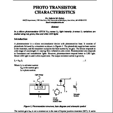
Photo Transistor 2u3g6r
December 2021 0
Spice Model For A Photo Transistor 4a563m
December 2021 0
Transistor 6m4b1i
December 2019 62
Transistor 6m4b1i
May 2022 0
Transistor 6m4b1i
December 2019 130More Documents from "Ck L" l2y4o
Photo Transistor 2u3g6r
December 2021 0
Hw5 Mastering Physics Solution 492o3q
November 2021 0
Form 3 Science 6s514i
December 2019 51
Energy And Momentum 554n22
December 2021 0
Hw2 Mastering Physics Solution 611949
November 2019 54