Lnk364pn 1k3p2l
This document was ed by and they confirmed that they have the permission to share it. If you are author or own the copyright of this book, please report to us by using this report form. Report r6l17
Overview 4q3b3c
& View Lnk364pn as PDF for free.
More details 26j3b
- Words: 999
- Pages: 2
DI-133 Design Idea LinkSwitch-XT ®
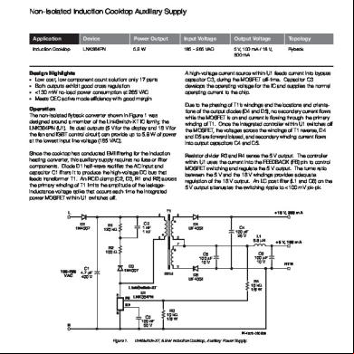
Non-Isolated Induction Cooktop Auxiliary Supply
Application
Device
Power Output
Input Voltage
Output Voltage
Topology
Induction Cooktop
LNK364PN
5.9 W
185 – 265 VAC
5 V, 100 mA / 18 V, 300 mA
Flyback
Design Highlights • Low cost, low component count solution: only 17 parts • Both outputs exhibit good cross regulation • <130 mW no-load power consumption at 265 VAC • Meets CEC active mode efficiency with good margin
A high-voltage current source within U1 feeds current into by capacitor C3, during the MOSFET off-time. Capacitor C3 develops the operating voltage for the IC and supplies the normal operating current to the chip. Due to the phasing of T1’s windings and the locations and orientations of the output diodes (D4 and D5), no secondary current flows while the MOSFET is on and current is flowing through the primary winding of T1. Once the integrated controller within U1 switches off the MOSFET, the voltages across the windings of T1 reverse, D4 and D5 are forward biased, and secondary winding current flows into output capacitors C4 and C5.
Operation The non-isolated flyback converter shown in Figure 1 was designed around a member of the LinkSwitch-XT IC family, the LNK364PN (U1). Its dual outputs (5 V for the display and 18 V for the fan and IGBT control circuit) can provide up to 5.9 W of power at the lowest input line voltage (185 VAC). Since the cooktop has conducted EMI filtering for the induction heating converter, this auxiliary supply requires no fuse or filter components. Diode D1 half-wave rectifies the AC input and capacitor C1 filters it to produce the high-voltage DC bus that feeds transformer T1. An RCD clamp (C2, D3, R1 and R2) across the primary winding of T1 limits the amplitude of the leakageinductance voltage spike that occurs each time the integrated power MOSFET within U1 switches off.
Resistor divider R3 and R4 sense the 5 V output. The controller within U1 uses the current into the (FB) pin to control MOSFET switching and regulate the 5 V output. The turns ratio between the 5 V and the 18 V windings provides adequate regulation of the 18 V output. An LC post filter (L1 and C6) on the 5 V output attenuates the switching ripple to <100 mV pk-pk.
T1
L
2
D1 1N4007
C2 1 nF 1 kV
R1 120 kΩ
+18 V, 300 mA
8
D4 UF4002 3
6
C4 100 μF 25 V
7
R2 100 Ω
185-265 VAC
C6 100 μF 10 V
C5 100 μF 10 V 5
D3 1N4007
C1 4.7 μF 400 V
D
L1 6.8 μH
EE16
D5 UF4002
+5 V, 100 mA
RTN
R4 16 kΩ 1/8 W
LinkSwitch-XT U1 FB LNK364PN BP
S
C3 100 nF 50 V
N
R3 10 kΩ 1/8 W
PI-4573-010208
Figure 1.
www.powerint.com
LinkSwitch-XT, 5.9 W Induction Cooktop, Auxiliary Power Supply.
January 2008
Key Design Points • Wind T1 for the lowest leakage inductance by choosing wire gauge sizes that completely fill each winding layer. • The PI Xls spreadsheet tool can be used to modify this supply to allow operation over the universal AC input voltage range (85 – 265 VAC).
•
•
PI-4583-021407
No-Load Input Power (mW)
130
Loading
5 V Output
18 V Output
100% on 5 V and 100% on 18 V
4.94
18.14
110
100% on 5 V and 10% on 18 V
5.01
19.46
100
10% on 5 V and 100% on 18 V
5.08
17.99
90
10% on 5 V and 10% on 18 V
5.14
18.51
120
Table 1. Output Cross Regulation at 265 VAC.
80 70
205
185
225
245
265
Input Voltage (VAC) Figure 2.
No-Load Input Power vs. Line Voltage.
PI-4584-021407
73
Efficiency (%)
Select the values of R3 and R4 so that when the 5 V output is in regulation, there is 1.63 V on the FB pin, with a current of 49 μA flowing into the FB pin. Higher ohmic values for R3 and R4 will not improve efficiency and may degrade regulation accuracy. resistor R4 must be connected before the LC post (L1 and C6) filter in order to avoid groups of enabled and disabled switching cycles from occurring.
72
Full Load 71
Transformer Parameters Core Material
EE16 NC-2H or equivalent, gapped for ALG of 63 nH/t²
Bobbin
EE16, 8 pin
Winding Details
Primary: 200T, 36 AWG, tape Secondary: 5 V:, 11T, 29 AWG triple insulated, tape Secondary: 18 V: 26T, 30 AWG triple insulated, tape
Primary Inductance 2.77 mH, ±10% Primary Resonant Frequency
500 kHz (minimum)
Leakage Inductance
111 μH (maximum)
Table 2. Transformer Parameters. (AWG = American Wire Gauge, TIW = Triple Insulated Wire)
70
205
185
225
245
265
Input Voltage (V) Figure 3.
Efficiency vs. Input Voltage at Full Load.
Power Integrations 5245 Hellyer Avenue San Jose, CA 95138, USA. Main: +1 408-414-9200 Customer Service Phone: +1-408-414-9665 Fax: +1-408-414-9765 Email: [email protected]
Power Integrations reserves the right to make changes to its products at any time to improve reliability or manufacturability. Power Integrations does not assume any liability arising from the use of any device or circuit described herein. POWER INTEGRATIONS MAKES NO WARRANTY HEREIN AND SPECIFICALLY DISCLAIMS ALL WARRANTIES INCLUDING, WITHOUT LIMITATION, THE IMPLIED WARRANTIES OF MERCHANTABILITY, FITNESS FOR A PARTICULAR PURPOSE, AND NON-INFRINGEMENT OF THIRD PARTY RIGHTS. The products and applications illustrated herein (transformer construction and circuits external to the products) may be covered by one or more U.S. and foreign patents or potentially by pending U.S. and foreign patent applications assigned to Power Integrations. A complete list of Power Integrations' patents may be found at www.powerint.com. Power Integrations grants its customers a license under certain patent rights as set forth at http://www.powerint.com/ip.htm.
On the Web www.powerint.com
The PI logo, TOPSwitch, TinySwitch, LinkSwitch, DPA-Switch, PeakSwitch, EcoSmart, Clampless, E-Shield, Filterfuse, StackFET, PI Expert and PI FACTS are trademarks of Power Integrations, Inc. Other trademarks are property of their respective companies. ©2007, Power Integrations, Inc.
B 1/08
DI-133
Related Documents 171j1w
Lnk364pn 1k3p2l
October 2021 0More Documents from "Jose Benavides" 54g
Datasheet Str-g6653.pdf 4e295d
November 2019 93
Fan7529 (ic601) - Datasheet Ii 3xq4e
November 2019 82
Datasheet A1357-nte2513 (c3420-nte2514) 24a6d
April 2023 0
Lnk364pn 1k3p2l
October 2021 0
2c82t
December 2020 0