Irfp1405 1d3zo
This document was ed by and they confirmed that they have the permission to share it. If you are author or own the copyright of this book, please report to us by using this report form. Report r6l17
Overview 4q3b3c
& View Irfp1405 as PDF for free.
More details 26j3b
- Words: 2,094
- Pages: 9
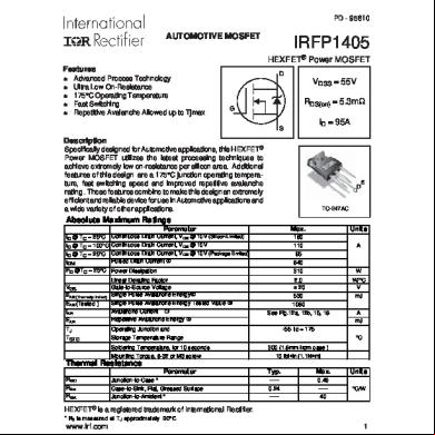
PD - 95810
AUTOMOTIVE MOSFET
IRFP1405 HEXFET® Power MOSFET
Features ● ● ● ● ●
Advanced Process Technology Ultra Low On-Resistance 175°C Operating Temperature Fast Switching Repetitive Avalanche Allowed up to Tjmax
D
VDSS = 55V RDS(on) = 5.3mΩ
G
ID = 95A
S
Description Specifically designed for Automotive applications, this HEXFET® Power MOSFET utilizes the latest processing techniques to achieve extremely low on-resistance per silicon area. Additional features of this design are a 175°C junction operating temperature, fast switching speed and improved repetitive avalanche rating . These features combine to make this design an extremely efficient and reliable device for use in Automotive applications and a wide variety of other applications.
S
D G TO-247AC
Absolute Maximum Ratings ID @ TC = 25°C ID @ TC = 100°C ID @ TC = 25°C IDM PD @TC = 25°C
Parameter
Max.
Continuous Drain Current, VGS @ 10V (Silicon Limited) Continuous Drain Current, VGS @ 10V Continuous Drain Current, VGS @ 10V (Package Limited) Pulsed Drain Current
160 110 95 640 310
c
Power Dissipation
VGS EAS (Thermally limited) EAS (Tested ) IAR EAR
Linear Derating Factor Gate-to-Source Voltage Single Pulse Avalanche Energy Single Pulse Avalanche Energy Tested Value Avalanche Current Repetitive Avalanche Energy
TJ TSTG
Operating Junction and Storage Temperature Range
d
c
h
g
Soldering Temperature, for 10 seconds Mounting Torque, 6-32 or M3 screw
Parameter Junction-to-Case * Case-to-Sink, Flat, Greased Surface Junction-to-Ambient *
A
W
2.0 ± 20 530 1060 See Fig.12a, 12b, 15, 16
W/°C V mJ A mJ
-55 to + 175 °C 300 (1.6mm from case ) 10 lbf in (1.1N m)
y
Thermal Resistance RθJC Rθcs RθJA
Units
y
Typ.
Max.
Units
––– 0.24 –––
0.49 ––– 40
°C/W
HEXFET® is a ed trademark of International Rectifier. * Rθ is measured at TJ approximately 90°C
www.irf.com
1 12/22/03
IRFP1405
Electrical Characteristics @ TJ = 25°C (unless otherwise specified) Parameter
V(BR)DSS
Drain-to-Source Breakdown Voltage
Min. Typ. Max. Units 55
–––
–––
∆V(BR)DSS/∆TJ
Breakdown Voltage Temp. Coefficient
–––
0.058
–––
RDS(on)
Static Drain-to-Source On-Resistance
–––
4.2
5.3
VGS(th)
Gate Threshold Voltage
2.0
–––
4.0
gfs IDSS
Forward Transconductance
V
Conditions VGS = 0V, ID = 250µA
V/°C Reference to 25°C, ID = 1mA mΩ VGS = 10V, ID = 95A
e
V
VDS = VGS, ID = 250µA VDS = 25V, ID = 95A
77
–––
–––
S
–––
–––
20
µA
–––
–––
250
Gate-to-Source Forward Leakage
–––
–––
200
Gate-to-Source Reverse Leakage
–––
–––
-200
Qg
Total Gate Charge
–––
120
180
Qgs
Gate-to-Source Charge
–––
30
–––
Qgd
Gate-to-Drain ("Miller") Charge
–––
53
–––
VGS = 10V
td(on)
Turn-On Delay Time
–––
12
–––
VDD = 28V
tr
Rise Time
–––
160
–––
td(off)
Turn-Off Delay Time
–––
140
–––
tf
Fall Time
–––
150
–––
VGS = 10V
LD
Internal Drain Inductance
–––
5.0
–––
Between lead,
LS
Internal Source Inductance
–––
13
–––
6mm (0.25in.) from package and center of die VGS = 0V
IGSS
Drain-to-Source Leakage Current
VDS = 55V, VGS = 0V VDS = 55V, VGS = 0V, TJ = 125°C
nA
VGS = 20V VGS = -20V ID = 95A
nC
VDS = 44V
e
ID = 95A ns
nH
RG = 2.6 Ω
e D
G
S
Ciss
Input Capacitance
–––
5600
–––
Coss
Output Capacitance
–––
1310
–––
Crss
Reverse Transfer Capacitance
–––
350
–––
Coss
Output Capacitance
–––
6550
–––
VGS = 0V, VDS = 1.0V, ƒ = 1.0MHz
Coss
Output Capacitance
–––
920
–––
VGS = 0V, VDS = 44V, ƒ = 1.0MHz
Coss eff.
Effective Output Capacitance
–––
1750
–––
VGS = 0V, VDS = 0V to 44V
VDS = 25V pF
ƒ = 1.0MHz
f
Source-Drain Ratings and Characteristics Parameter
Min. Typ. Max. Units
IS
Continuous Source Current
–––
–––
95
ISM
(Body Diode) Pulsed Source Current
–––
–––
640
VSD
(Body Diode) Diode Forward Voltage
–––
–––
1.3
V
trr
Reverse Recovery Time
–––
70
110
ns
Qrr
Reverse Recovery Charge
–––
170
260
nC
ton
Forward Turn-On Time
c
Conditions MOSFET symbol
A
showing the integral reverse p-n junction diode. TJ = 25°C, IS = 95A, VGS = 0V
e
TJ = 25°C, IF = 95A, VDD = 28V di/dt = 100A/µs
e
Intrinsic turn-on time is negligible (turn-on is dominated by LS+LD)
Notes:
„ Coss eff. is a fixed capacitance that gives the same charging time max. junction temperature. (See fig. 11). as Coss while VDS is rising from 0 to 80% VDSS . ‚ Limited by TJmax, starting TJ = 25°C, L = 0.12mH … Limited by TJmax , see Fig.12a, 12b, 15, 16 for typical repetitive R G = 25Ω, IAS = 95A, VGS =10V. Part not avalanche performance. recommended for use above this value. † This value determined from sample failure population. 100% ƒ Pulse width ≤ 1.0ms; duty cycle ≤ 2%. tested to this value in production. Repetitive rating; pulse width limited by
2
www.irf.com
IRFP1405 1000
1000
100 BOTTOM
TOP
4.5V
10
≤ 60µs PULSE WIDTH Tj = 25°C
ID, Drain-to-Source Current (A)
ID, Drain-to-Source Current (A)
TOP
VGS 15V 10V 8.0V 7.0V 6.0V 5.5V 5.0V 4.5V
BOTTOM
100
4.5V
1
≤ 60µs PULSE WIDTH Tj = 175°C
10 0.1
1
10
100
0.1 0
VDS, Drain-to-Source Voltage (V)
11
10 10
100 100
VDS, Drain-to-Source Voltage (V)
Fig 1. Typical Output Characteristics
Fig 2. Typical Output Characteristics
140
1000
T J = 25°C
Gfs, Forward Transconductance (S)
ID, Drain-to-Source Current (Α)
VGS 15V 10V 8.0V 7.0V 6.0V 5.5V 5.0V 4.5V
T J = 175°C
100
VDS = 25V ≤ 60µs PULSE WIDTH
T J = 25°C
120 100 80
T J = 175°C 60 40 20
VDS = 10V 380µs PULSE WIDTH
10 4.0
5.0
6.0
7.0
8.0
9.0
VGS, Gate-to-Source Voltage (V)
Fig 3. Typical Transfer Characteristics
www.irf.com
10.0
0 0
20
40
60
80
100
ID, Drain-to-Source Current (A)
Fig 4. Typical Forward Transconductance Vs. Drain Current
3
IRFP1405 10000
ID= 95A VGS, Gate-to-Source Voltage (V)
8000
C, Capacitance (pF)
20
VGS = 0V, f = 1 MHZ C iss = C gs + C gd, C ds SHORTED C rss = C gd C oss = C ds + C gd
Ciss
6000
4000
Coss 2000
VDS= 44V VDS= 28V
16
12
8
4 FOR TEST CIRCUIT SEE FIGURE 13
Crss 0
0 1
10
0
100
40
80
120
160
200
QG Total Gate Charge (nC)
VDS, Drain-to-Source Voltage (V)
Fig 6. Typical Gate Charge Vs. Gate-to-Source Voltage
Fig 5. Typical Capacitance Vs. Drain-to-Source Voltage
10000
1000.0
ID, Drain-to-Source Current (A)
ISD, Reverse Drain Current (A)
OPERATION IN THIS AREA LIMITED BY R DS(on)
T J = 175°C
100.0
10.0 T J = 25°C 1.0
1000
100
100µsec
10
1
Tc = 25°C Tj = 175°C Single Pulse
VGS = 0V
10msec DC
0.1
0.1 0.2
0.6
1.0
1.4
1.8
VSD, Source-toDrain Voltage (V)
Fig 7. Typical Source-Drain Diode Forward Voltage
4
1msec
2.2
1
10
100
1000
VDS , Drain-toSource Voltage (V)
Fig 8. Maximum Safe Operating Area
www.irf.com
IRFP1405 200 RDS(on) , Drain-to-Source On Resistance (Normalized)
2.5
ID , Drain Current (A)
LIMITED BY PACKAGE
150
100
50
0 25
50
75
100
125
150
ID = 95A VGS = 10V 2.0
1.5
1.0
0.5
175
-60 -40 -20
T C , Case Temperature (°C)
0
20 40 60 80 100 120 140 160 180
T J , Junction Temperature (°C)
Fig 10. Normalized On-Resistance Vs. Temperature
Fig 9. Maximum Drain Current Vs. Case Temperature
1
Thermal Response ( Z thJC )
D = 0.50 0.1
0.20 0.10 0.05 0.02 0.01
0.01
τJ
R1 R1 τJ τ1
R2 R2 τC τ2
τ1
τ2
τ
Ri (°C/W) τi (sec) 0.2529 0.00080 0.2368 0.014283
Ci= τi/Ri Ci i/Ri
0.001
SINGLE PULSE ( THERMAL RESPONSE )
Notes: 1. Duty Factor D = t1/t2 2. Peak Tj = P dm x Zthjc + Tc
0.0001 1E-006
1E-005
0.0001
0.001
0.01
0.1
t1 , Rectangular Pulse Duration (sec)
Fig 11. Maximum Effective Transient Thermal Impedance, Junction-to-Case
www.irf.com
5
IRFP1405
DRIVER
L
VDS
D.U.T
RG
+ V - DD
IAS 20V VGS
tp
A
0.01Ω
Fig 12a. Unclamped Inductive Test Circuit V(BR)DSS tp
EAS, Single Pulse Avalanche Energy (mJ)
2000
15V
ID 16A 20A BOTTOM 95A TOP
1500
1000
500
0 25
50
75
100
125
150
175
Starting T J, Junction Temperature (°C) I AS
Fig 12c. Maximum Avalanche Energy Vs. Drain Current
Fig 12b. Unclamped Inductive Waveforms QG
10 V QGD
4.0
VG
Charge
Fig 13a. Basic Gate Charge Waveform
L VCC
VGS(th) Gate threshold Voltage (V)
QGS
3.5
3.0
ID = 250µA
2.5
2.0
DUT
0
1.5
1K
-75 -50 -25
0
25
50
75
100 125 150 175
T J , Temperature ( °C )
Fig 13b. Gate Charge Test Circuit
6
Fig 14. Threshold Voltage Vs. Temperature
www.irf.com
IRFP1405
Avalanche Current (A)
10000
Duty Cycle = Single Pulse
1000
Allowed avalanche Current vs avalanche pulsewidth, tav assuming ∆ Tj = 25°C due to avalanche losses. Note: In no case should Tj be allowed to exceed Tjmax
0.01
100
0.05 0.10
10
1 1.0E-06
1.0E-05
1.0E-04
1.0E-03
1.0E-02
1.0E-01
tav (sec)
Fig 15. Typical Avalanche Current Vs.Pulsewidth
EAR , Avalanche Energy (mJ)
600
TOP Single Pulse BOTTOM 1% Duty Cycle ID = 95A
500
400
300
200
100
0 25
50
75
100
125
150
Starting T J , Junction Temperature (°C)
Fig 16. Maximum Avalanche Energy Vs. Temperature
www.irf.com
Notes on Repetitive Avalanche Curves , Figures 15, 16: (For further info, see AN-1005 at www.irf.com) 1. Avalanche failures assumption: Purely a thermal phenomenon and failure occurs at a temperature far in excess of T jmax. This is validated for every part type. 2. Safe operation in Avalanche is allowed as long asTjmax is not exceeded. 3. Equation below based on circuit and waveforms shown in Figures 12a, 12b. 4. PD (ave) = Average power dissipation per single avalanche pulse. 5. BV = Rated breakdown voltage (1.3 factor s for voltage increase during avalanche). 6. I av = Allowable avalanche current. 7. ∆T = Allowable rise in junction temperature, not to exceed Tjmax (assumed as 25°C in Figure 15, 16). tav = Average time in avalanche. 175 D = Duty cycle in avalanche = tav ·f ZthJC(D, tav ) = Transient thermal resistance, see figure 11) PD (ave) = 1/2 ( 1.3·BV·Iav) = DT/ ZthJC Iav = 2DT/ [1.3·BV·Zth] EAS (AR) = PD (ave)·tav
7
IRFP1405
D.U.T
Driver Gate Drive
+
ƒ +
‚
„
• • • •
D.U.T. ISD Waveform Reverse Recovery Current
+
dv/dt controlled by RG Driver same type as D.U.T. I SD controlled by Duty Factor "D" D.U.T. - Device Under Test
P.W. Period
*
RG
D=
VGS=10V
Circuit Layout Considerations • Low Stray Inductance • Ground Plane • Low Leakage Inductance Current Transformer
-
-
Period
P.W.
VDD
+
Body Diode Forward Current di/dt D.U.T. VDS Waveform Diode Recovery dv/dt
Re-Applied Voltage
-
Body Diode
VDD
Forward Drop
Inductor Curent Ripple ≤ 5%
ISD
* VGS = 5V for Logic Level Devices Fig 17. Peak Diode Recovery dv/dt Test Circuit for N-Channel HEXFET® Power MOSFETs
V DS VGS RG
RD
D.U.T. +
-VDD
10V Pulse Width ≤ 1 µs Duty Factor ≤ 0.1 %
Fig 18a. Switching Time Test Circuit VDS 90%
10% VGS td(on)
tr
t d(off)
tf
Fig 18b. Switching Time Waveforms
8
www.irf.com
IRFP1405 TO-247AC Package Outline Dimensions are shown in millimeters
'5* 1†
TO-247AC Part Marking Information
Notes: T his part marking information applies to devices produced before 02/26/2001 or for parts manufactured in GB.
EXAMPLE: THIS IS AN IRFPE30 WITH ASS EMBLY LOT CODE 3A1Q
INTERNAT IONAL RECTIFIER LOGO
PART NUMBER IRF PE30
3A1Q
9302
DATE CODE (YYWW) YY = YEAR WW = WEEK
AS S EMBLY LOT CODE
Notes : T his part marking information applies to devices produced after 02/26/2001 EXAMPLE: THIS IS AN IRFPE30 WITH ASS EMBLY LOT CODE 5657 AS SEMBLED ON WW 35, 2000 IN T HE AS S EMBLY LINE "H"
INTERNATIONAL RECTIFIER LOGO AS SEMB LY LOT CODE
PART NUMBER IRFPE 30 56
035H 57
DATE CODE YEAR 0 = 2000 WEEK 35 LINE H
TO-247AC packages are not recommended for Surface Mount Application. Data and specifications subject to change without notice. This product has been designed and qualified for Automotive [Q101] market. Qualification Standards can be found on IR’s Web site.
IR WORLD HEADQUARTERS: 233 Kansas St., El Segundo, California 90245, USA Tel: (310) 252-7105 TAC Fax: (310) 252-7903 Visit us at www.irf.com for sales information.12/03
www.irf.com
9
Related Documents 171j1w
Irfp1405 1d3zo
August 2022 0More Documents from "Cah Ngaloef" 1r37p
Irfp1405 1d3zo
August 2022 0
Alesis Ra300 Schematics 2q291a
January 2022 0
Tutorial Face Making In Blender 6p386s
April 2020 28
January 2021 0
Sk Pedoman Pelayanan Kefarmasian 174r34
May 2020 2