Buck–boost Converter - Wikipedia 3z5l6l
This document was ed by and they confirmed that they have the permission to share it. If you are author or own the copyright of this book, please report to us by using this report form. Report r6l17
Overview 4q3b3c
& View Buck–boost Converter - Wikipedia as PDF for free.
More details 26j3b
- Words: 2,304
- Pages: 8
11/3/2016
Buck–boost converter Wikipedia
Buck–boost converter From Wikipedia, the free encyclopedia
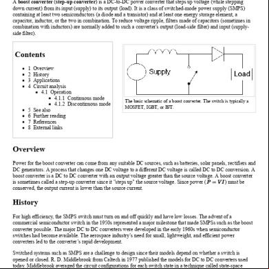
The buck–boost converter is a type of DCtoDC converter that has an output voltage magnitude that is either greater than or less than the input voltage magnitude. It is equivalent to a flyback converter using a single inductor instead of a transformer.[1] Two different topologies are called buck–boost converter. Both of them can produce a range of output voltages, ranging from much larger (in absolute magnitude) than the input voltage, down to almost zero.
The basic schematic of an inverting buck–boost converter.
The inverting topology The output voltage is of the opposite polarity than the input. This is a switchedmode power supply with a similar circuit topology to the boost converter and the buck converter. The output voltage is adjustable based on the duty cycle of the switching transistor. One possible drawback of this converter is that the switch does not have a terminal at ground; this complicates the driving circuitry. Another drawback is of any consequence if the power supply is isolated from the load circuit (if, for example, the supply is a battery) because the supply and diode polarity can simply be reversed. The switch can be on either the ground side or the supply side. A buck (stepdown) converter combined with a boost (stepup) converter The output voltage is typically of the same polarity of the input, and can be lower or higher than the input. Such a noninverting buckboost converter may use a single inductor which is used for both the buck inductor mode and the boost inductor mode, using switches instead of diodes,[2][3][4] sometimes called a "fourswitch buckboost converter",[5] it may use multiple inductors but only a single switch as in the SEPIC and Ćuk topologies.
Contents 1 Principle of operation of the 4switch topology 2 Principle of operation of the inverting topology 2.1 Conceptual overview 2.2 Continuous mode 2.3 Discontinuous mode 2.4 Limit between continuous and discontinuous modes 3 Nonideal circuit 3.1 Effect of parasitic resistances 4 See also 5 References 6 Further reading
Principle of operation of the 4switch topology The 4switch converter combines the buck and boost converters. It can operate in either the buck or the boost mode. In either mode, only one switch controls the duty cycle, another is for commutation and must be operated inversely to the former one, and the remaining two switches are in a fixed position. It seems that you could also build a 2switch buckboost converter with the two diodes, but upgrading the diodes to FET transistor switches doesn't cost much extra while due to lower voltage drop the efficiency improves. https://en.wikipedia.org/wiki/Buck%E2%80%93boost_converter
1/8
11/3/2016
Buck–boost converter Wikipedia
Principle of operation of the inverting topology The basic principle of the inverting buck–boost converter is fairly simple (see figure 2): while in the Onstate, the input voltage source is directly connected to the inductor (L). This results in accumulating energy in L. In this stage, the capacitor supplies energy to the output load. while in the Offstate, the inductor is connected to the output load and capacitor, so energy is transferred from L to C and R. Compared to the buck and boost converters, the characteristics of the inverting buck–boost converter are mainly: polarity of the output voltage is opposite to that of the input; the output voltage can vary continuously from 0 to (for an ideal converter). The output voltage ranges for a buck and a boost converter are respectively to 0 and to .
Conceptual overview Like the buck and boost converters, the operation of the buckboost is best understood in of the inductor's "reluctance" to allow rapid change in current. From the initial state in which nothing is charged and the switch is open, the current through the inductor is zero. When the switch is first closed, the blocking diode prevents current from flowing into the right hand side of the circuit, so it must all flow through the inductor. However, since the inductor doesn't like rapid current change, it will initially keep the current low by dropping most of the voltage provided by the source. Over time, the inductor will allow the current to slowly increase by decreasing its voltage drop. Also during this time, the inductor will store energy in the form of a magnetic field.
The basics of the 4switch topology
Continuous mode If the current through the inductor L never falls to zero during a commutation cycle, the converter is said to operate in continuous mode. The current and voltage waveforms in an ideal converter can be seen in Figure 3.
Fig. 1: Schematic of a buck–boost converter.
From to , the converter is in OnState, so the switch S is closed. The rate of change in the inductor current (IL) is therefore given by
At the end of the Onstate, the increase of IL is therefore:
https://en.wikipedia.org/wiki/Buck%E2%80%93boost_converter
2/8
11/3/2016
Buck–boost converter Wikipedia
D is the duty cycle. It represents the fraction of the commutation period T during which the switch is On. Therefore D ranges between 0 (S is never on) and 1 (S is always on). During the Offstate, the switch S is open, so the inductor current flows through the load. If we assume zero voltage drop in the diode, and a capacitor large enough for its voltage to remain constant, the evolution of IL is:
Therefore, the variation of IL during the Offperiod is:
As we consider that the converter operates in steadystate conditions, the amount of energy stored in each of its components has to be the same at the beginning and at the end of a commutation cycle. As the energy in an inductor is given by:
Fig. 2: The two operating states of a buck–boost converter: When the switch is turned on, the input voltage source supplies current to the inductor, and the capacitor supplies current to the resistor (output load). When the switch is opened, the inductor supplies current to the load via the diode D.
it is obvious that the value of IL at the end of the Off state must be the same with the value of IL at the beginning of the Onstate, i.e. the sum of the variations of IL during the on and the off states must be zero:
Substituting yields:
and
by their expressions
Fig 3: Waveforms of current and voltage in a buck–boost converter operating in continuous mode.
This can be written as:
This in return yields that:
https://en.wikipedia.org/wiki/Buck%E2%80%93boost_converter
3/8
11/3/2016
Buck–boost converter Wikipedia
From the above expression it can be seen that the polarity of the output voltage is always negative (because the duty cycle goes from 0 to 1), and that its absolute value increases with D, theoretically up to minus infinity when D approaches 1. Apart from the polarity, this converter is either stepup (a boost converter) or stepdown (a buck converter). Thus it is named a buck–boost converter.
Discontinuous mode In some cases, the amount of energy required by the load is small enough to be transferred in a time smaller than the whole commutation period. In this case, the current through the inductor falls to zero during part of the period. The only difference in the principle described above is that the inductor is completely discharged at the end of the commutation cycle (see waveforms in figure 4). Although slight, the difference has a strong effect on the output voltage equation. It can be calculated as follows: Because the inductor current at the beginning of the cycle is zero, its maximum value (at ) is
During the offperiod, IL falls to zero after δ.T:
Fig 4: Waveforms of current and voltage in a buck–boost converter operating in discontinuous mode.
Using the two previous equations, δ is:
The load current is equal to the average diode current ( ). As can be seen on figure 4, the diode current is equal to the inductor current during the offstate. Therefore, the output current can be written as:
Replacing
and δ by their respective expressions yields:
Therefore, the output voltage gain can be written as:
https://en.wikipedia.org/wiki/Buck%E2%80%93boost_converter
4/8
11/3/2016
Buck–boost converter Wikipedia
Compared to the expression of the output voltage gain for the continuous mode, this expression is much more complicated. Furthermore, in discontinuous operation, the output voltage not only depends on the duty cycle, but also on the inductor value, the input voltage and the output current...
Limit between continuous and discontinuous modes As told at the beginning of this section, the converter operates in discontinuous mode when low current is drawn by the load, and in continuous mode at higher load current levels. The limit between discontinuous and continuous modes is reached when the inductor current falls to zero exactly at the end of the commutation cycle. with the notations of figure 4, this corresponds to :
In this case, the output current (output current at the limit between continuous and discontinuous modes) is given by: Fig 5: Evolution of the normalized output voltage with the normalized output current in a buck–boost converter.
Replacing by the expression given in the discontinuous mode section yields:
As is the current at the limit between continuous and discontinuous modes of operations, it satisfies the expressions of both modes. Therefore, using the expression of the output voltage in continuous mode, the previous expression can be written as:
Let's now introduce two more notations: the normalized voltage, defined by
. It corresponds to the gain in voltage of the converter;
\scriptstyle is equal to the maximum increase of the {\frac inductor current during a cycle; i.e., the increase of the inductor current with a duty cycle D=1. So, in steady state operation of the converter, this means that equals 0 for no output current, and 1 for the maximum current the converter can deliver. the normalized current, defined by
. The term
Using these notations, we have: in continuous mode,
; \scriptstyle \left|V_{o}\right|=
https://en.wikipedia.org/wiki/Buck%E2%80%93boost_converter in discontinuous mode, ;
5/8
11/3/2016
Buck–boost converter Wikipedia
\scriptstyle ; \left|V_{o}\right|= the current at the limit between continuous and discontinuous mode is in discontinuous mode,
\scriptstyle . I_{{o_{{{\text{lim}}}}}}= Therefore the locus of the limit between continuous and discontinuous modes is given by \scriptstyle. {\frac {1} These expressions have been plotted in figure 5. The difference in behavior between the continuous and discontinuous modes can be seen clearly.
Nonideal circuit Effect of parasitic resistances In the analysis above, no dissipative elements (resistors) have been considered. That means that the power is transmitted without losses from the input voltage source to the load. However, parasitic resistances exist in all circuits, due to the resistivity of the materials they are made from. Therefore, a fraction of the power managed by the converter is dissipated by these parasitic resistances. For the sake of simplicity, we consider here that the inductor is the only nonideal component, and that it is equivalent to an inductor and a resistor in series. This assumption is acceptable because an inductor is made of one long wound piece of wire, so it is likely to exhibit a nonnegligible parasitic resistance (RL). Furthermore, current flows through the inductor both in the on and the off states. Using the statespace averaging method, we can write:
Fig 6: Evolution of the output voltage of a buck– boost converter with the duty cycle when the parasitic resistance of the inductor increases.
V_{i}={\bar V}_{{{\text{L}}}}+ where and are respectively the average voltage across the inductor and the switch over the commutation cycle. If we consider that the converter operates in steadystate, the average current through the inductor is constant. The average voltage across the inductor is: {\bar V}_{{{\text{L}}}}=L{\frac {{\bar When the switch is in the onstate, \scriptstyle . When it is off, the diode is forward biased (we consider the continuous mode operation), therefore . Therefore, the average voltage across the switch is:
The output current is the opposite of the inductor current during the offstate. the average inductor current is therefore:
https://en.wikipedia.org/wiki/Buck%E2%80%93boost_converter
6/8
11/3/2016
Buck–boost converter Wikipedia
Assuming the output current and voltage have negligible ripple, the load of the converter can be considered purely resistive. If R is the resistance of the load, the above expression becomes:
Using the previous equations, the input voltage becomes:
This can be written as:
If the inductor resistance is zero, the equation above becomes equal to the one of the ideal case. But when RL increases, the voltage gain of the converter decreases compared to the ideal case. Furthermore, the influence of RL increases with the duty cycle. This is summarized in figure 6.
See also Ćuk converter SEPIC converter
References 1. The Flyback Converter (http://ecee.colorado.edu/~ecen4517/materials/flyback.pdf) Lecture notes ECEN4517 Department of Electrical and Computer Engineering University of Colorado, Boulder. 2. "Noninverting BuckBoost Regulator" (p.9) (http://ecee.colorado.edu/copec/book/slides/Ch6slides.pdf) 3. ST AN2389: "An MCUbased low cost noninverting buckboost converter for battery chargers" (http://www.st.com/stw ebui/static/active/en/resource/technical/document/application_note/CD00116928.pdf) 4. Motorola Semiconductor. "Application note AN954: A Unique Converter Configuration provides stepup/down functions" (http://www.datasheetarchive.com/dataframe.php?file=DSA457120.pdf&dir=Datasheets23&part=AN954). 1985. "... a unique stepup/down configuration can be created ... which still employs a single inductor for the voltage transformation." 5. Haifeng Fan. "Wide VIN and HighPower Challenges with BuckBoost Converters" (http://powerelectronics.com/dcdcc onverters/widevinandhighpowerchallengesbuckboostconverters). 2015.
Further reading Daniel W. Hart, "Introduction to Power Electronics", Prentice Hall, Upper Saddle River, New Jersey USA, 1997 ISBN 0 023511826 Christophe Basso, SwitchMode Power Supplies: SPICE Simulations and Practical Designs. McGrawHill. ISBN 007 1508589.
Retrieved from "https://en.wikipedia.org/w/index.php?title=Buck– boost_converter&oldid=745755348"
https://en.wikipedia.org/wiki/Buck%E2%80%93boost_converter
Wikimedia Commons has media related to Buckboost converters. 7/8
11/3/2016
Buck–boost converter Wikipedia
Categories: Electric power conversion Voltage regulation This page was last modified on 23 October 2016, at 03:19. Text is available under the Creative Commons AttributionShareAlike License; additional may apply. By using this site, you agree to the of Use and Privacy Policy. Wikipedia® is a ed trademark of the Wikimedia Foundation, Inc., a nonprofit organization.
https://en.wikipedia.org/wiki/Buck%E2%80%93boost_converter
8/8
Buck–boost converter Wikipedia
Buck–boost converter From Wikipedia, the free encyclopedia
The buck–boost converter is a type of DCtoDC converter that has an output voltage magnitude that is either greater than or less than the input voltage magnitude. It is equivalent to a flyback converter using a single inductor instead of a transformer.[1] Two different topologies are called buck–boost converter. Both of them can produce a range of output voltages, ranging from much larger (in absolute magnitude) than the input voltage, down to almost zero.
The basic schematic of an inverting buck–boost converter.
The inverting topology The output voltage is of the opposite polarity than the input. This is a switchedmode power supply with a similar circuit topology to the boost converter and the buck converter. The output voltage is adjustable based on the duty cycle of the switching transistor. One possible drawback of this converter is that the switch does not have a terminal at ground; this complicates the driving circuitry. Another drawback is of any consequence if the power supply is isolated from the load circuit (if, for example, the supply is a battery) because the supply and diode polarity can simply be reversed. The switch can be on either the ground side or the supply side. A buck (stepdown) converter combined with a boost (stepup) converter The output voltage is typically of the same polarity of the input, and can be lower or higher than the input. Such a noninverting buckboost converter may use a single inductor which is used for both the buck inductor mode and the boost inductor mode, using switches instead of diodes,[2][3][4] sometimes called a "fourswitch buckboost converter",[5] it may use multiple inductors but only a single switch as in the SEPIC and Ćuk topologies.
Contents 1 Principle of operation of the 4switch topology 2 Principle of operation of the inverting topology 2.1 Conceptual overview 2.2 Continuous mode 2.3 Discontinuous mode 2.4 Limit between continuous and discontinuous modes 3 Nonideal circuit 3.1 Effect of parasitic resistances 4 See also 5 References 6 Further reading
Principle of operation of the 4switch topology The 4switch converter combines the buck and boost converters. It can operate in either the buck or the boost mode. In either mode, only one switch controls the duty cycle, another is for commutation and must be operated inversely to the former one, and the remaining two switches are in a fixed position. It seems that you could also build a 2switch buckboost converter with the two diodes, but upgrading the diodes to FET transistor switches doesn't cost much extra while due to lower voltage drop the efficiency improves. https://en.wikipedia.org/wiki/Buck%E2%80%93boost_converter
1/8
11/3/2016
Buck–boost converter Wikipedia
Principle of operation of the inverting topology The basic principle of the inverting buck–boost converter is fairly simple (see figure 2): while in the Onstate, the input voltage source is directly connected to the inductor (L). This results in accumulating energy in L. In this stage, the capacitor supplies energy to the output load. while in the Offstate, the inductor is connected to the output load and capacitor, so energy is transferred from L to C and R. Compared to the buck and boost converters, the characteristics of the inverting buck–boost converter are mainly: polarity of the output voltage is opposite to that of the input; the output voltage can vary continuously from 0 to (for an ideal converter). The output voltage ranges for a buck and a boost converter are respectively to 0 and to .
Conceptual overview Like the buck and boost converters, the operation of the buckboost is best understood in of the inductor's "reluctance" to allow rapid change in current. From the initial state in which nothing is charged and the switch is open, the current through the inductor is zero. When the switch is first closed, the blocking diode prevents current from flowing into the right hand side of the circuit, so it must all flow through the inductor. However, since the inductor doesn't like rapid current change, it will initially keep the current low by dropping most of the voltage provided by the source. Over time, the inductor will allow the current to slowly increase by decreasing its voltage drop. Also during this time, the inductor will store energy in the form of a magnetic field.
The basics of the 4switch topology
Continuous mode If the current through the inductor L never falls to zero during a commutation cycle, the converter is said to operate in continuous mode. The current and voltage waveforms in an ideal converter can be seen in Figure 3.
Fig. 1: Schematic of a buck–boost converter.
From to , the converter is in OnState, so the switch S is closed. The rate of change in the inductor current (IL) is therefore given by
At the end of the Onstate, the increase of IL is therefore:
https://en.wikipedia.org/wiki/Buck%E2%80%93boost_converter
2/8
11/3/2016
Buck–boost converter Wikipedia
D is the duty cycle. It represents the fraction of the commutation period T during which the switch is On. Therefore D ranges between 0 (S is never on) and 1 (S is always on). During the Offstate, the switch S is open, so the inductor current flows through the load. If we assume zero voltage drop in the diode, and a capacitor large enough for its voltage to remain constant, the evolution of IL is:
Therefore, the variation of IL during the Offperiod is:
As we consider that the converter operates in steadystate conditions, the amount of energy stored in each of its components has to be the same at the beginning and at the end of a commutation cycle. As the energy in an inductor is given by:
Fig. 2: The two operating states of a buck–boost converter: When the switch is turned on, the input voltage source supplies current to the inductor, and the capacitor supplies current to the resistor (output load). When the switch is opened, the inductor supplies current to the load via the diode D.
it is obvious that the value of IL at the end of the Off state must be the same with the value of IL at the beginning of the Onstate, i.e. the sum of the variations of IL during the on and the off states must be zero:
Substituting yields:
and
by their expressions
Fig 3: Waveforms of current and voltage in a buck–boost converter operating in continuous mode.
This can be written as:
This in return yields that:
https://en.wikipedia.org/wiki/Buck%E2%80%93boost_converter
3/8
11/3/2016
Buck–boost converter Wikipedia
From the above expression it can be seen that the polarity of the output voltage is always negative (because the duty cycle goes from 0 to 1), and that its absolute value increases with D, theoretically up to minus infinity when D approaches 1. Apart from the polarity, this converter is either stepup (a boost converter) or stepdown (a buck converter). Thus it is named a buck–boost converter.
Discontinuous mode In some cases, the amount of energy required by the load is small enough to be transferred in a time smaller than the whole commutation period. In this case, the current through the inductor falls to zero during part of the period. The only difference in the principle described above is that the inductor is completely discharged at the end of the commutation cycle (see waveforms in figure 4). Although slight, the difference has a strong effect on the output voltage equation. It can be calculated as follows: Because the inductor current at the beginning of the cycle is zero, its maximum value (at ) is
During the offperiod, IL falls to zero after δ.T:
Fig 4: Waveforms of current and voltage in a buck–boost converter operating in discontinuous mode.
Using the two previous equations, δ is:
The load current is equal to the average diode current ( ). As can be seen on figure 4, the diode current is equal to the inductor current during the offstate. Therefore, the output current can be written as:
Replacing
and δ by their respective expressions yields:
Therefore, the output voltage gain can be written as:
https://en.wikipedia.org/wiki/Buck%E2%80%93boost_converter
4/8
11/3/2016
Buck–boost converter Wikipedia
Compared to the expression of the output voltage gain for the continuous mode, this expression is much more complicated. Furthermore, in discontinuous operation, the output voltage not only depends on the duty cycle, but also on the inductor value, the input voltage and the output current...
Limit between continuous and discontinuous modes As told at the beginning of this section, the converter operates in discontinuous mode when low current is drawn by the load, and in continuous mode at higher load current levels. The limit between discontinuous and continuous modes is reached when the inductor current falls to zero exactly at the end of the commutation cycle. with the notations of figure 4, this corresponds to :
In this case, the output current (output current at the limit between continuous and discontinuous modes) is given by: Fig 5: Evolution of the normalized output voltage with the normalized output current in a buck–boost converter.
Replacing by the expression given in the discontinuous mode section yields:
As is the current at the limit between continuous and discontinuous modes of operations, it satisfies the expressions of both modes. Therefore, using the expression of the output voltage in continuous mode, the previous expression can be written as:
Let's now introduce two more notations: the normalized voltage, defined by
. It corresponds to the gain in voltage of the converter;
\scriptstyle is equal to the maximum increase of the {\frac inductor current during a cycle; i.e., the increase of the inductor current with a duty cycle D=1. So, in steady state operation of the converter, this means that equals 0 for no output current, and 1 for the maximum current the converter can deliver. the normalized current, defined by
. The term
Using these notations, we have: in continuous mode,
; \scriptstyle \left|V_{o}\right|=
https://en.wikipedia.org/wiki/Buck%E2%80%93boost_converter in discontinuous mode, ;
5/8
11/3/2016
Buck–boost converter Wikipedia
\scriptstyle ; \left|V_{o}\right|= the current at the limit between continuous and discontinuous mode is in discontinuous mode,
\scriptstyle . I_{{o_{{{\text{lim}}}}}}= Therefore the locus of the limit between continuous and discontinuous modes is given by \scriptstyle. {\frac {1} These expressions have been plotted in figure 5. The difference in behavior between the continuous and discontinuous modes can be seen clearly.
Nonideal circuit Effect of parasitic resistances In the analysis above, no dissipative elements (resistors) have been considered. That means that the power is transmitted without losses from the input voltage source to the load. However, parasitic resistances exist in all circuits, due to the resistivity of the materials they are made from. Therefore, a fraction of the power managed by the converter is dissipated by these parasitic resistances. For the sake of simplicity, we consider here that the inductor is the only nonideal component, and that it is equivalent to an inductor and a resistor in series. This assumption is acceptable because an inductor is made of one long wound piece of wire, so it is likely to exhibit a nonnegligible parasitic resistance (RL). Furthermore, current flows through the inductor both in the on and the off states. Using the statespace averaging method, we can write:
Fig 6: Evolution of the output voltage of a buck– boost converter with the duty cycle when the parasitic resistance of the inductor increases.
V_{i}={\bar V}_{{{\text{L}}}}+ where and are respectively the average voltage across the inductor and the switch over the commutation cycle. If we consider that the converter operates in steadystate, the average current through the inductor is constant. The average voltage across the inductor is: {\bar V}_{{{\text{L}}}}=L{\frac {{\bar When the switch is in the onstate, \scriptstyle . When it is off, the diode is forward biased (we consider the continuous mode operation), therefore . Therefore, the average voltage across the switch is:
The output current is the opposite of the inductor current during the offstate. the average inductor current is therefore:
https://en.wikipedia.org/wiki/Buck%E2%80%93boost_converter
6/8
11/3/2016
Buck–boost converter Wikipedia
Assuming the output current and voltage have negligible ripple, the load of the converter can be considered purely resistive. If R is the resistance of the load, the above expression becomes:
Using the previous equations, the input voltage becomes:
This can be written as:
If the inductor resistance is zero, the equation above becomes equal to the one of the ideal case. But when RL increases, the voltage gain of the converter decreases compared to the ideal case. Furthermore, the influence of RL increases with the duty cycle. This is summarized in figure 6.
See also Ćuk converter SEPIC converter
References 1. The Flyback Converter (http://ecee.colorado.edu/~ecen4517/materials/flyback.pdf) Lecture notes ECEN4517 Department of Electrical and Computer Engineering University of Colorado, Boulder. 2. "Noninverting BuckBoost Regulator" (p.9) (http://ecee.colorado.edu/copec/book/slides/Ch6slides.pdf) 3. ST AN2389: "An MCUbased low cost noninverting buckboost converter for battery chargers" (http://www.st.com/stw ebui/static/active/en/resource/technical/document/application_note/CD00116928.pdf) 4. Motorola Semiconductor. "Application note AN954: A Unique Converter Configuration provides stepup/down functions" (http://www.datasheetarchive.com/dataframe.php?file=DSA457120.pdf&dir=Datasheets23&part=AN954). 1985. "... a unique stepup/down configuration can be created ... which still employs a single inductor for the voltage transformation." 5. Haifeng Fan. "Wide VIN and HighPower Challenges with BuckBoost Converters" (http://powerelectronics.com/dcdcc onverters/widevinandhighpowerchallengesbuckboostconverters). 2015.
Further reading Daniel W. Hart, "Introduction to Power Electronics", Prentice Hall, Upper Saddle River, New Jersey USA, 1997 ISBN 0 023511826 Christophe Basso, SwitchMode Power Supplies: SPICE Simulations and Practical Designs. McGrawHill. ISBN 007 1508589.
Retrieved from "https://en.wikipedia.org/w/index.php?title=Buck– boost_converter&oldid=745755348"
https://en.wikipedia.org/wiki/Buck%E2%80%93boost_converter
Wikimedia Commons has media related to Buckboost converters. 7/8
11/3/2016
Buck–boost converter Wikipedia
Categories: Electric power conversion Voltage regulation This page was last modified on 23 October 2016, at 03:19. Text is available under the Creative Commons AttributionShareAlike License; additional may apply. By using this site, you agree to the of Use and Privacy Policy. Wikipedia® is a ed trademark of the Wikimedia Foundation, Inc., a nonprofit organization.
https://en.wikipedia.org/wiki/Buck%E2%80%93boost_converter
8/8
Related Documents 171j1w
Boost Converter - Wikipedia 2g6rn
November 2019 46
Catalytic Converter - Wikipedia 6x385n
November 2019 73
Torque Converter - Wikipedia 4d2g11
December 2019 65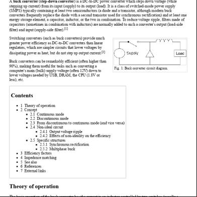
Buck Converter - Wikipedia, The Free Encyclopedia 36723g
December 2019 58
Catalytic Converter - Wikipedia, The Free Encyclopedia 1x4e5
November 2019 33
Matrix Converter 5l3d29
November 2021 0More Documents from "Sudip Mondal" 3f2w61

Dual Trace Oscilloscope 1b6t6q
May 2023 0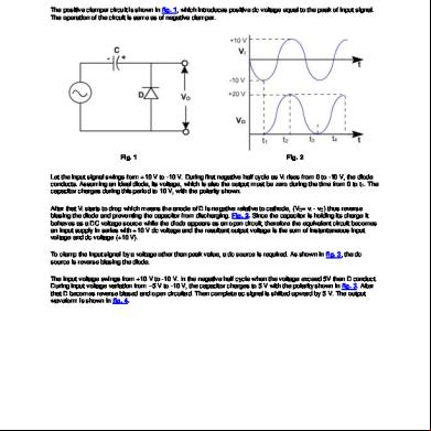
Positive Clamper 45705i
March 2023 0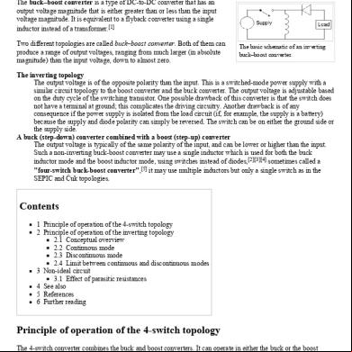
2c82t
November 2019 60
Boost Converter - Wikipedia 2g6rn
November 2019 46
Microwave Transistor Amplifiers Analysis And Design 3va33
October 2019 67