Dac1220 j1z58
This document was ed by and they confirmed that they have the permission to share it. If you are author or own the copyright of this book, please report to us by using this report form. Report r6l17
Overview 4q3b3c
& View Dac1220 as PDF for free.
More details 26j3b
- Words: 8,759
- Pages: 26
DA
DAC1220
C1
220
www.ti.com...................................................................................................................................... SBAS082G – FEBRUARY 1998 – REVISED SEPTEMBER 2009
20-Bit, Low-Power Digital-to-Analog Converter Check for Samples: DAC1220
FEATURES
DESCRIPTION
•
The DAC1220 is a 20-bit digital-to-analog (D/A) converter offering 20-bit monotonic performance over the specified temperature range. It utilizes delta-sigma technology to achieve inherently linear performance in a small package at very low power. The resolution of the device can be programmed to 20 bits for Full-Scale, settling to 0.003% within 15ms typical, or 16 bits for Full-Scale, settling to 0.012% within 2ms max. The output range is two times the external reference voltage. On-chip calibration circuitry dramatically reduces low offset and gain errors.
1
2
• • • • •
20-Bit Monotonicity Ensured Over –40°C to +85°C Low Power: 2.5mW Voltage Output Settling Time: 2ms to 0.012% Maximum Linearity Error: ±0.0015% On-Chip Calibration
APPLICATIONS • • • • •
Process Control ATE Pin Electronics Closed-Loop Servo Control Smart Transmitters Portable Instruments
The DAC1220 features a synchronous serial interface; in single-converter applications, the serial interface can be accomplished with just two wires, allowing low-cost isolation. For multiple converters, a CS signal allows for selection of the appropriate D/A converter. The DAC1220 has been designed for closed-loop control applications in the industrial process control market and high-resolution applications in the test and measurement market. It is also ideal for remote applications, battery-powered instruments, and isolated systems. The DAC1220 is available in an SSOP-16 package.
XIN
XOUT
VREF
AVDD
AGND
Clock Generator
Microcontroller 2nd−Order ∆Σ Modulator
Instruction Command Data Offset Full−Scale
SDIO SCLK
2nd−Order Continuous Time Post Filter
C1 VOUT C2
Modulator Control
Serial Interface
CS
1st−Order Switched Capacitor Filter
DVDD
DGND
1
2
Please be aware that an important notice concerning availability, standard warranty, and use in critical applications of Texas Instruments semiconductor products and disclaimers thereto appears at the end of this data sheet. All trademarks are the property of their respective owners.
PRODUCTION DATA information is current as of publication date. Products conform to specifications per the of the Texas Instruments standard warranty. Production processing does not necessarily include testing of all parameters.
Copyright © 1998–2009, Texas Instruments Incorporated
DAC1220 SBAS082G – FEBRUARY 1998 – REVISED SEPTEMBER 2009...................................................................................................................................... www.ti.com
This integrated circuit can be damaged by ESD. Texas Instruments recommends that all integrated circuits be handled with appropriate precautions. Failure to observe proper handling and installation procedures can cause damage. ESD damage can range from subtle performance degradation to complete device failure. Precision integrated circuits may be more susceptible to damage because very small parametric changes could cause the device not to meet its published specifications.
PACKAGE/ORDERING INFORMATION For the most current package and ordering information see the Package Option Addendum at the end of this document, or see the TI web site at www.ti.com.
ABSOLUTE MAXIMUM RATINGS (1) Over operating free-air temperature range (unless otherwise noted). DAC1220
UNIT
AVDD to DVDD
±0.3
V
AVDD to AGND
–0.3 to +6
V
DVDD to DGND
–0.3 to +6
V
AGND to DGND
±0.3
V
+2.0 to +3.0
V
Digital input voltage to DGND
–0.3 to DVDD + 0.3
V
Digital output voltage to DGND
–0.3 to DVDD + 0.3
V
Package power dissipation
(TJmax – TA) / θ JA
W
+150
°C
200
°C/W
+300
°C
VREF voltage to AGND
Maximum junction temperature (TJmax) Thermal resistance, θ JA Lead temperature (soldering, 10s) (1)
2
SSOP-16
Stresses beyond those listed under absolute maximum ratings may cause permanent damage to the device. These are stress ratings only, and functional operation of the device at these or any other conditions beyond those indicated under the Electrical Characteristics is not implied. Exposure to absolute maximum rated conditions for extended periods may affect device reliability.
Submit Documentation
Copyright © 1998–2009, Texas Instruments Incorporated
Product Folder Link(s): DAC1220
DAC1220 www.ti.com...................................................................................................................................... SBAS082G – FEBRUARY 1998 – REVISED SEPTEMBER 2009
ELECTRICAL CHARACTERISTICS All specifications at TMIN to TMAX, AVDD = DVDD = +5V, fXIN = 2.5MHz, VREF = +2.5V, and 16-bit mode, unless otherwise noted. DAC1220E PARAMETER
CONDITIONS
MIN
TYP
MAX
UNIT
ACCURACY Monotonicity
16
Monotonicity
20-bit mode
Bits
20
Bits
Linearity error
±15 (1)
ppm of FSR
±60
ppm of FSR
Unipolar offset error and gain error (2) Unipolar offset error drift (3)
1
Bipolar zero offset error (2)
VOUT = VREF
ppm/°C
±15
Bipolar zero offset drift (3)
ppm of FSR
1
ppm/°C
Gain error (2)
±150
Gain error drift (3) Power-supply rejection ratio (PSRR)
at DC, dB = –20log(ΔVOUT/ΔVDD)
ppm of FSR
2
ppm/°C
60
dB
ANALOG OUTPUT Output voltage (4)
0
2 × VREF
Output current
0.5
V mA
Capacitive load
500
pF
Short-circuit current
±20
mA
Short-circuit duration
GND or VDD
Indefinite
DYNAMIC PERFORMANCE Settling time (5) Output noise voltage
To ±0.012%
1.8
20-bit mode, to ±0.003%
15
2
ms ms
0.1Hz to 10Hz
1
μVRMS
REFERENCE INPUT Input voltage
2.25
Input impedance
2.5
2.75
100
V kΩ
DIGITAL INPUT/OUTPUT Logic family
TTL-compatible CMOS
Logic levels (all except XIN) VIH
2.0
DVDD + 0.3
V
VIL
–0.3
0.8
V
VOH
IOH = –0.8mA
VOL
IOL = 1.6mA
3.6
V
Input-leakage current XIN frequency range (fXIN) Data format
0.5 -programmable
0.4
V
±10
μA
2.5
MHz
Offset binary two's complement or straight binary
POWER-SUPPLY REQUIREMENTS Power-supply voltage
4.75
5.25
V
Supply current Analog current
360
μA
Digital current
140
μA
460
μA
Analog current (1) (2) (3) (4) (5)
20-bit mode
Valid from AGND + 20mV to AVDD – 20mV. Applies after calibration. Recalibration can remove these errors. Ideal output voltage; does not take into gain and offset error. Valid from AGND + 20mV to AVDD – 20mV. Outside of this range, settling time can be twice the value indicated. For 16-bit mode, C1 = 2.2nF, C2 = 0.22nF; for 20-bit mode, C1 = 10nF, C2 = 3.3nF. Submit Documentation
Copyright © 1998–2009, Texas Instruments Incorporated
Product Folder Link(s): DAC1220
3
DAC1220 SBAS082G – FEBRUARY 1998 – REVISED SEPTEMBER 2009...................................................................................................................................... www.ti.com
ELECTRICAL CHARACTERISTICS (continued) All specifications at TMIN to TMAX, AVDD = DVDD = +5V, fXIN = 2.5MHz, VREF = +2.5V, and 16-bit mode, unless otherwise noted. DAC1220E PARAMETER
CONDITIONS
MIN
TYP
MAX
UNIT
POWER-SUPPLY REQUIREMENTS, continued Digital current
20-bit mode
μA
140
Power dissipation
2.5
3.5
mW
20-bit mode
3.0
mW
Sleep mode
0.45
mW
TEMPERATURE RANGE Specified performance
–40
+85
°C
DEVICE INFORMATION DVDD
1
16
SCLK
XOUT
2
15
SDIO
XIN
3
14
CS
DGND
4
13
AGND
DAC1220E AVDD
5
12
VREF
DNC
6
11
VOUT
DNC
7
10
C2
DNC
8
9
C1
PIN DESCRIPTIONS
4
PIN
NAME
1
DVDD
Digital supply, +5V nominal
DESCRIPTION
2
XOUT
System clock output (for crystal)
3
XIN
4
DGND
Digital ground
5
AVDD
Analog supply, +5V nominal
6
DNC
Do not connect
7
DNC
Do not connect
8
DNC
Do not connect
System clock input
9
C1
Filter capacitor (see text)
10
C2
Filter capacitor (see text)
11
VOUT
Analog output voltage
12
VREF
Reference input
13
AGND
Analog ground
14
CS
Chip-select input
15
SDIO
Serial data input/output
16
SCLK
Clock input for serial data transfer
Submit Documentation
Copyright © 1998–2009, Texas Instruments Incorporated
Product Folder Link(s): DAC1220
DAC1220 www.ti.com...................................................................................................................................... SBAS082G – FEBRUARY 1998 – REVISED SEPTEMBER 2009
TYPICAL CHARACTERISTICS At TA = +25°C, AVDD = DVDD = +5.0V, fXIN = 2.5MHz, VREF = 2.5V, C1 = 2.2nF, and calibrated mode, unless otherwise specified. POWER-SUPPLY REJECTION RATIO vs FREQUENCY
LARGE-SIGNAL SETTLING TIME
60
5.0 4.5 4.0 3.5
40
3.0 (V)
PSRR (dB)
50
30
2.5 2.0
20
1.5 1.0
400mVPP Ripple Mid−Range Output
10
0.5
0
0 10
100
1k
10k
0
1
2
Frequency (Hz)
3
4
Time (ms)
Figure 1.
Figure 2.
OUTPUT NOISE VOLTAGE vs FREQUENCY
LINEARITY ERROR vs CODE
10k
10 −40°C 8 Linearity Error (ppm)
Noise (nV/√Hz)
1k
100
10
+25°C +85°C
6 4 2 0
1
2 10
100
1k
10k
100k
1M
0
Frequency (Hz)
10k
20k
30k
40k
50k
60k
70k
Code
Figure 3.
Figure 4.
Submit Documentation
Copyright © 1998–2009, Texas Instruments Incorporated
Product Folder Link(s): DAC1220
5
DAC1220 SBAS082G – FEBRUARY 1998 – REVISED SEPTEMBER 2009...................................................................................................................................... www.ti.com
THEORY OF OPERATION The DAC1220 is a monolithic 20-bit delta-sigma (ΔΣ) digital-to-analog converter (DAC) designed for applications requiring extremely high precision. The delta-sigma topology used in the DAC1220 ensures 20-bit monotonicity over the industrial temperature range. The DAC1220 can also be operated in 16-bit mode, which gives a faster settling time at the expense of higher noise. The core of the DAC1220 consists of an interpolation filter and a second-order delta-sigma modulator. The output of the modulator is ed to a first-order switched-capacitor filter in series with a second-order continuous-time filter, which generates the output voltage. To increase settling time, the DAC1220 can adjust its filter cutoff frequency when it detects a voltage output step of greater than approximately 40mV. This behavior can be disabled. An onboard self-calibration facility compensates for internal offset and gain errors. Calibration values may be stored and loaded externally if desired. The DAC1220 can be put into a sleep mode, in which power consumption is cut by about 1/6 to approximately 0.45mW. In sleep mode, the output is disconnected.
Self-Calibration System The self-calibration system of the DAC1220 measures the DAC output and calculates appropriate gain and offset calibration constants. The output changes during calibration, but can optionally be disconnected during the procedure. Offset calibration is performed by setting the DAC output voltage to mid-scale and repeatedly comparing the DAC output to the VREF voltage using an auto-zeroed comparator, which is re-zeroed after every comparison. The comparator results are recorded and averaged, two’s complement adjusted, and placed in the Offset Calibration . Gain calibration is performed in a similar way, except that the correction is done against an internally-generated reference voltage, and the final value is calculated differently. The Full-Scale Calibration result represents the gain code and is not two’s complement adjusted. Changing the Gain value can change the range of voltages that are output for the same digital codes, centered on VREF.
BASIC CONNECTIONS A schematic showing basic connections to the DAC1220 is given in Figure 5.
The DAC1220 is controlled using a synchronous serial interface, using either two or three wires. The interface may be operated bidirectionally or unidirectionally; readback is optional. +5V 4.7µF Ceramic
12pF(1) 2.5MHz
DVDD
SCLK
SPI CLOCK
XOUT
SDIO
SPI DATA
XIN 12pF(1)
DGND +5V
4.7µF Ceramic
From Chip Select or Ground
CS AGND
AVDD
VREF
DNC
VOUT
DNC
C2
DNC
C1
+2.5V from Voltage Reference C2(2)
VOUT C1
(2)
NOTES: (1) Depends on crystal and board layout. (2) See text for recommended values.
Figure 5. DAC1220 Schematic
6
Submit Documentation
Copyright © 1998–2009, Texas Instruments Incorporated
Product Folder Link(s): DAC1220
DAC1220 www.ti.com...................................................................................................................................... SBAS082G – FEBRUARY 1998 – REVISED SEPTEMBER 2009
Output
Digital Connections
The output voltage range is nominally 0V to 2 × VREF. It does not go below ground. The output amplifier is not designed for heavy loads; it can drive a maximum of 0.5mA. At power-on and during sleep mode, the amplifier is disconnected, so the output is high impedance.
The digital lines, except for the crystal oscillator lines, operate at TTL-compatible CMOS logic levels. They can be driven from 3.3V logic sources.
The output is not fully linear to the rails; maximum linearity is specified from (AGND + 20mV) to (AVDD – 20mV). For linearity from 0–5V, AVDD can be increased to 5.02V or more, and AGND can be decreased to –20mV or less. As long as the specified operating limits are observed, this will not damage the device.
Filter Capacitors The continuous-time output filter requires two external capacitors to operate. The recommended values of these capacitors depend on whether the DAC1220 will be operated in 16-bit or 20-bit mode, and are shown in Table 1. Table 1. Filter Capacitor Values CAPACITOR
16-BIT MODE
20-BIT MODE
C1
2.2nF
10nF
C2
0.22nF
3.3nF
The capacitors should be stable and high grade. Film types, or other capacitors designed for precision filtering, are strongly recommended. Low-quality capacitors will degrade performance significantly. The C1 and C2 pins are very sensitive. It is critical to surround them with a guard ring at the reference voltage for best noise performance. See the Layout section for more information.
Voltage Reference
In noise-sensitive applications, it may be helpful to keep the level transition rates on the digital lines slow. Fast transitions can couple through the device to the output, causing noise. Rate limiting can be done with resistance or even an RC filter.
Clock Oscillator The DAC1220 has a built-in crystal oscillator at pins XIN and XOUT. To use it, connect a crystal and load capacitors as shown in Figure 5. 12pF load capacitors are shown in the schematic, but the correct value depends mainly on the crystal and layout, and not on the oscillator itself. Load capacitance affects startup time, oscillation frequency, and reliability. If startup is unreliable, try lowering the capacitor values. that parasitic board and pin capacitance can be a significant portion of the crystal load capacitance. When the crystal oscillator is operating, a sinusoidal signal of relatively low amplitude will be observed at both the XIN and XOUT pins. The typical frequency to use with the DAC1220 is 2.5MHz. Deviating too far from this may alter noise and settling time, as well as timing characteristics.
Connecting an External Clock An external clock signal can be connected at XIN. A CMOS or TTL logic signal can be used. If an external clock signal is used, XOUT should be left unconnected. In some cases, an RC filter on the clock line may reduce noise.
The voltage reference input is designed for +2.5V. At this voltage, the output will range from ground to approximately 5V, as noted above.
Submit Documentation
Copyright © 1998–2009, Texas Instruments Incorporated
Product Folder Link(s): DAC1220
7
DAC1220 SBAS082G – FEBRUARY 1998 – REVISED SEPTEMBER 2009...................................................................................................................................... www.ti.com
Serial Interface The DAC1220 can be operated from most SPI peripherals, or it can be bit-banged. Note that if SDIO is operated bidirectionally, it may be necessary to place a pullup resistor on the line, so that the line will not be floating. The serial clock is limited to one-tenth of the master clock frequency. For a 2.4576MHz master clock, the serial clock may be no faster than 245.76kHz. The designer should bear this in mind, as it may prevent the DAC1220 from being shared with other SPI devices or placed on an SPI bus, which may run much faster. If the DAC1220 is placed on a shared SPI bus, the chip-select line must be controlled; otherwise, it can be grounded. Although the SDIO line is bidirectional, it can be operated as an input only, as long as no reads are performed. The DAC1220 can be operated without reads, although for situations requiring high reliability, this is not recommended, since the device s and operation cannot be directly verified.
Power Supplies The DAC1220 has separate analog and digital power supply connections. Both are intended to operate at +5V. The digital supply must never exceed the analog supply by more than 300mV. If it does, the DAC1220 may be permanently damaged. The analog supply may be greater than the digital supply without damage, however.
Most designs will use a single power supply for AVDD and DVDD. In these designs, the supplies ramp simultaneously, which is acceptable. In those designs that use separate sources for AVDD and DVDD, the two supplies must be sequenced properly. This is easily done using a Schottky diode, as shown in Figure 6. The diode ensures that DVDD will not exceed AVDD by more than a Schottky diode drop.
Brownouts and Power-On Reset The DAC1220 incorporates a power-on reset (POR) circuit. The circuit will trigger as long as the power supply ramps up at 50mV/ms or faster. If the power supply ramps more slowly than this, the POR may not trigger. The DAC1220 does not have a brownout detector. The POR circuit will not retrigger unless the supply voltages have approached ground. Because of this, if the supply falls to a low voltage, it may corrupt the logic of the DAC1220, causing it to operate erratically or to fail entirely. It may be necessary to forcibly discharge the supply, since the DAC1220 may occasionally fail to detect the SCLK reset pattern in this condition. The SCLK reset pattern serves in place of a reset pin. See the SCLK Reset Pattern section for information.
Supply Decoupling Both supply pins should be heavily decoupled at the device for best performance. A 10μF multi-layer ceramic capacitor can be used for this, or a tantalum capacitor in parallel with a small (0.1μF) ceramic capacitor can be used. Both capacitors, particularly the ceramic capacitor, should be placed as close to the pins as possible being decoupled.
5V Digital Supply
DVDD
5V Analog Supply
AVDD
Figure 6. Supply Sequence Protection
8
Submit Documentation
Copyright © 1998–2009, Texas Instruments Incorporated
Product Folder Link(s): DAC1220
DAC1220 www.ti.com...................................................................................................................................... SBAS082G – FEBRUARY 1998 – REVISED SEPTEMBER 2009
DIGITAL INTERFACE Timing The serial interface is synchronous and controlled by the SCLK input. The DAC1220 latches incoming bits on the falling edge of SCLK, and shifts outgoing bits on the rising edge of SCLK. An external interface should shift outgoing bits on the rising edge of SCLK, and latch incoming bits on the falling edge of SCLK. The relevant waveforms are illustrated in the timing diagrams (see Figure 7 to Figure 11). Timing numbers are given in Table 2 through Table 4. tXIN t1
t2
XIN
Figure 7. XIN Clock Timing Table 2. XIN Timing Characteristics SYMBOL
DESCRIPTION
fXIN
XIN clock frequency
tXIN
XIN clock period
MIN
MAX
UNITS
1
NOM
2.5
MHz
400
1000
ns
t1
XIN clock high
0.4 × tXIN
ns
t2
XIN clock low
0.4 × tXIN
ns
t3 t4
t5
SCLK t6
t7
SDIO t8
Figure 8. Serial Input/Output Timing Table 3. Serial I/O Timing Characteristics SYMBOL
DESCRIPTION
MIN
NOM
MAX
UNITS
t3
SCLK high
5 × tXIN
ns
t4
SCLK low
5 × tXIN
ns
t5
Data in valid to SCLK falling edge (setup)
40
ns
t6
SCLK falling edge to data in not valid (hold)
20
ns
t7
Data out valid to rising edge of SCLK (hold)
0
t8
SCLK rising edge to new data out valid (delay)
ns 50
ns
Submit Documentation
Copyright © 1998–2009, Texas Instruments Incorporated
Product Folder Link(s): DAC1220
9
DAC1220 SBAS082G – FEBRUARY 1998 – REVISED SEPTEMBER 2009...................................................................................................................................... www.ti.com t9
t14
SCLK IN7
SDIO
IN1
IN0
INM
IN1
IN0
IN7
OUT1
OUT0
IN7
Write Data SDIO
IN7
IN1
IN0
OUTM
Read Data
Figure 9. Serial Interface Timing (CS Low) t15 CS t 10
t10
t9
SCLK IN7
SDIO
IN1
IN0
INM
IN1
IN0
IN7
OUTM
OUT1
OUT0
IN7
Write Data IN7
SDIO
IN1
IN0
Read Data
Figure 10. Serial Interface Timing (Using CS)
CS
SCLK
t11
t 10
t12 t13
SDIO
IN7
IN0
OUT MSB
OUT0
t9 SDIO is an input
SDIO is an output
Figure 11. SDIO Input to Output Transition Timing Table 4. Serial Interface Timing Characteristics SYMBOL
10
DESCRIPTION
MIN
NOM
MAX
UNITS
t9
Falling edge of last SCLK for command to rising edge of first SCLK for data
13 × tXIN
ns
t10
Falling edge of CS to rising edge of SCLK
11 × tXIN
ns
t11
Falling edge of last SCLK for command to SDIO as output
8 × tXIN
t12
SDIO as output to rising edge of first SCLK for data
t13
Falling edge of last SCLK for data to SDIO tri-state
4 × tXIN
t14
Falling edge of last SCLK for data to rising edge of first SCLK of next command (CS tied low)
41 × tXIN
ns
t15
Rising edge of CS to falling edge of CS (using CS)
22 × tXIN
ns
10 × tXIN 4 × tXIN
Submit Documentation
ns ns
6 × tXIN
ns
Copyright © 1998–2009, Texas Instruments Incorporated
Product Folder Link(s): DAC1220
DAC1220 www.ti.com...................................................................................................................................... SBAS082G – FEBRUARY 1998 – REVISED SEPTEMBER 2009
The chip-select pin CS is active low. When CS is high, activity on SCLK is ignored. There are certain timing limits and delays which apply to the manipulation of CS, as shown in Figure 10. These must be observed, or the DAC1220 may malfunction. If CS is not used, it should be tied low. When CS is tied low, different timing limits and delays must be observed, as shown in Figure 9. If these are violated, the DAC1220 may malfunction. The serial interface is byte-oriented. All data is transferred in groups of eight bits.
I/O Recovery The DAC1220 has a timeout on the serial interface. If fCLK is 2.5MHz, the timeout is approximately 100ms. At 2.5MHz, if a command is interrupted, and no activity occurs on the SCLK or CS lines for 100ms, the DAC1220 will cancel the command. If the command was a write command, no s are affected.
SCLK Reset Pattern The DAC1220 does not have a dedicated reset pin. Instead, it contains a circuit which waits for a special pattern to appear on SCLK, and triggers the internal hardware reset line when it detects the special pattern. This pattern, called the SCLK reset pattern, is shown in Figure 12, with timing information given in Table 5. The pattern is very different from the usual clocking patterns which appear on SCLK, and is unlikely to be detected by accident during normal operation. The SCLK reset pattern can only be triggered when CS is low. When CS is high, the SCLK line is ignored, and the SCLK reset pattern is not detected.
The timeout period scales with the frequency of fCLK. Reset On Falling Edge t17
t 17
SCLK t16
t18
t19
Figure 12. Resetting the DAC1220 Table 5. Reset Timing Characteristics SYMBOL
DESCRIPTION
MIN 512 × tXIN
NOM
MAX
UNITS
800 × tXIN
ns
t16
First high period
t17
Low period
t18
Second high period
1024 × tXIN
1800 × tXIN
ns
t19
Third high period
2048 × tXIN
2400 × tXIN
ns
10 × tXIN
ns
Submit Documentation
Copyright © 1998–2009, Texas Instruments Incorporated
Product Folder Link(s): DAC1220
11
DAC1220 SBAS082G – FEBRUARY 1998 – REVISED SEPTEMBER 2009...................................................................................................................................... www.ti.com
PROGRAMMING Commands Communication with the DAC1220 consists entirely of commands, which access the DAC1220 s. Commands consist of a command byte followed by one, two or three data bytes. The data bytes can be sent to the DAC1220 or read from the DAC1220, depending on whether the command is a read command or a write command.
s
The format of the command byte is shown in Table 6, and the bits are described in Table 7. DAC1220 commands access the map, which is shown in Table 11. A DAC1220 command can read or write one byte, or two or three adjacent bytes, in the map.
Modes
Bit and Byte Order The order of the bits of data bytes in a command is configurable. The DAC1220 can be programmed to output data bytes MSB first or LSB first. The command byte is always transmitted MSB first. See the description of the MSB bit in Table 6 for further details. The order of the data bytes themselves is also configurable. See the description of the BD bit in Table 13 for details. Note that the BD bit does not affect the command byte; this always comes first.
There are four s in the DAC1220, as shown in the map in Table 11. The Data Input (DIR) and the two calibration s are 24 bits in length, and the Command (CMR), which contains configuration bits, is 16 bits in length.
The DAC1220 has three operating modes: Sleep, Normal, and Self Calibration. In Sleep mode, the DAC1220 output is off (high impedance), and much of the internal circuitry is switched off. In this mode the DAC1220 draws little power. The oscillator continues to run, however. Sleep is the mode entered after reset. In Normal mode, the DAC1220 is fully active, and the output is on. In Self Calibration mode, the DAC1220 runs its self-calibration sequence. After the sequence is complete, the DAC1220 switches to Normal mode. See the Calibration section for more information.
Table 6. Command Byte Format 7
6
R/W
5
4
MB
3
2
0
1
0
ADR
Table 7. Command Byte Bits BIT(S)
NAME
VALUE
7
R/W
0
Write to map
1
Read from map
6–5
MB
3–0
12
ADR
DESCRIPTION
Number of bytes to read or write 00b
1 byte
01b
2 bytes
10b
3 bytes
11b
Reserved; do not use
0–15
Start address in map
Submit Documentation
Copyright © 1998–2009, Texas Instruments Incorporated
Product Folder Link(s): DAC1220
DAC1220 www.ti.com...................................................................................................................................... SBAS082G – FEBRUARY 1998 – REVISED SEPTEMBER 2009
Startup Sequence At startup, the following procedure should generally be followed to properly initialize the DAC1220: 1. If the DAC1220 is being clocked from a crystal, wait for the oscillator to start—at least 25ms—before attempting to communicate with it. Trying to communicate with the DAC1220 before the crystal oscillator has reached its final frequency will usually result in corrupt communication. 2. Optionally apply the SCLK reset pattern. This should also only be done once the oscillator is started, since the pattern is detected using oscillator cycles. Applying the reset pattern at power-up ensures that the DAC1220 is reset properly, and not lingering in an unknown state in case of POR failure, brownout, etc. After a successful reset, the DAC1220 enters Normal mode. 3. Set up the Command as desired. This may include changing the mode from Sleep to Self Calibration or Normal. 4. Calibrate the DAC1220. Although this step is optional, the DAC1220 should almost always be calibrated. It is permissible to run calibration every time, or to use values from a previous calibration. See the Calibration section for details. After calibration, the DAC1220 returns to Normal mode. The DAC1220 is ready to accept data once it is in Normal mode, but calibration or the use of saved calibration values is highly recommended.
Calibration Calibration is governed by two s. The Offset Calibration (OCR) stores a value determining the offset calibration, and the Full-Scale Calibration (FCR) stores a value determining the gain calibration. The value in the OCR is scaled and additive. It has a linear relationship to the generated offset calibration voltage. The value in the FCR is scaled and multiplicative. It has a linear relationship to the generated gain calibration multiplier.
Since the calibration functions are linear, calibration results can be averaged for greater precision. For example, it may be beneficial to perform several self-calibrations in succession, record the result of each, average them together, and store the averages in the OCR and FCR.
Self-Calibration Procedure To perform a self-calibration, place the DAC1220 into Self Calibration mode by setting the MD1 bit to '0' and the MD0 bit to '1' in the Command . At a clock frequency of 2.5MHz, self-calibration takes between 300ms and 500ms; the actual time is indeterminate and depends on the results. If the CALPIN bit in the Command is '1', the output remains connected during calibration. The DAC voltage will change during the calibration process. This can be important if the DAC output is loaded significantly; disconnecting the output during calibration places a high load impedance on the output amplifier, which may be different from normal operation. If the CALPIN bit in the Command is '0', the output will be disconnected during calibration. If this is the case, when calibration begins, the DAC1220 briefly charges the C2 capacitor to the current output voltage. If the output is buffered, C2 effectively becomes a sample-and-hold capacitor, so that the final output voltage remains during calibration. When the calibration is complete, the DAC1220 switches to Normal mode. If the output was disconnected, it is reconnected at that time. The end of the calibration procedure can be detected by polling the MD1 and MD0 bits. When they become 0, the calibration is complete. If readback is not being performed, simply wait at least 500ms before sending further commands to the device, assuming that the clock frequency is 2.5MHz. Once calibration is complete, the OCR and FCR contain the results of the calibration, and the new constants are effective immediately.
Submit Documentation
Copyright © 1998–2009, Texas Instruments Incorporated
Product Folder Link(s): DAC1220
13
DAC1220 SBAS082G – FEBRUARY 1998 – REVISED SEPTEMBER 2009...................................................................................................................................... www.ti.com
Setting the Output Voltage To set the DAC1220 output voltage, write a code to the Data Input (DIR). A write to any of the bytes in the DIR causes the voltage to change at the completion of the write command. The DAC1220 operates in either 16- or 20-bit mode. The DIR is 24 bits wide, and the code stored in it is left justified, with the least significant bits ignored. Therefore, in 16-bit mode, only the upper 16 bits of the DIR are significant, and in 20-bit mode, only the upper 20 bits of the DIR are significant. In 20-bit mode, all three bytes of the DIR must be written to in order to completely update the code. In 16-bit mode, it is only necessary to write to the two upper bytes; a write to the lower byte has no effect on the output.
The code may be given in either straight binary or offset two's complement format. This is controlled by the DF bit in the Command (see the description in Table 13 for details). The two data format options and the 16- or 20-bit option give rise to four transfer functions, which are shown in Table 8. For reference, several ideal output voltages for given input codes are shown in Table 9. Note that the DIR code can also be considered a 24-bit number. This may be convenient in software. In this case the transfer functions for 16- and 20-bit modes are the same, except that in 16-bit mode the code is truncated by eight bits, and in 20-bit mode the code is truncated by four bits.
Table 8. Transfer Functions DATA FORMAT
20-BIT MODE
Offset two's complement
V OUT + 2VREF code)2 2 20
Straight binary
V OUT + 2VREF code 2 20
16-BIT MODE
19
V OUT + 2VREF code)2 2 16
15
V OUT + 2VREF code 2 16
Table 9. Example Output Voltages APPROXIMATE OUTPUT VOLTAGE
RESOLUTION 16-bit
0V 20-bit 16-bit 2.5V 20-bit 16-bit 5V 20-bit (1)
14
DATA FORMAT
CODE
DIR CONTENT
Two's complement
8000h
8000xxh
Straight binary
0000h
0000xxh
Two's complement
8000h
80000xh
Straight binary
0000h
00000xh
Two's complement
0000h
0000xxh
Straight binary
8000h
8000xxh
Two's complement
0000h
00000xh
Straight binary
8000h
80000xh
Two's complement
7FFFh
7FFFxxh
Straight binary
FFFFh
FFFFxxh
Two's complement
7FFFFh
7FFFFxh
Straight binary
FFFFFh
FFFFFxh
(1)
x = Do not care
Submit Documentation
Copyright © 1998–2009, Texas Instruments Incorporated
Product Folder Link(s): DAC1220
DAC1220 www.ti.com...................................................................................................................................... SBAS082G – FEBRUARY 1998 – REVISED SEPTEMBER 2009
Fast Settling Mode To speed up settling, the DAC1220 can change the cutoff frequency of its output filter. Raising the cutoff frequency causes the DAC1220 to settle faster, but at the expense of higher noise. The adaptive filtering mode provides a good compromise by increasing the filter frequency only while the DAC is changing its output by more than approximately 40mV. When the output has settled, the filter frequency is reduced again.
S
Adaptive filtering is controlled by the ADPT and DISF bits in the Command . The action of these bits together is described in Table 10. Table 10. Fast Settling Modes ADPT (CMR bit 15)
DISF (CMR bit 4)
0
0
The map is shown in Table 11. Table 11. Memory Map ADDRESS
FAST SETTLING MODE
CONTENT
0
DIR byte 2 (MSB)
1
DIR byte 1
2
DIR byte 0 (LSB)
3
Reserved
4
CMR byte 1 (MSB)
5
CMR byte 0 (LSB)
6
Reserved
7
Reserved
8
OCR byte 2 (MSB)
Fast settling only during > 40mV step
9
OCR byte 1
10
OCR byte 0 (LSB)
0
1
Disabled
11
Reserved
1
0
Fast settling always on (filter cutoff increased)
12
FCR byte 2 (MSB)
13
FCR byte 1
14
FCR byte 0 (LSB)
15
Reserved
1
1
Disabled
space Command (CMR)
The command contains the configuration bits of the DAC1220. It is shown in Table 12. The bits in the command are shown in Table 13. Writes to the CMR take effect at the negative edge of SCLK during the last bit of the last byte of the write command. blank Table 12. Command 15
14
13
12
11
10
9
8
ADPT
CALPIN
Reserved
Reserved
Reserved
R/W-0
R/W-0
R-1(1)
R-0
R-1
Reserved
CRST
Reserved
R-0
R/W-0
R-0
1
(1) In early versions of the DAC1220, this bit was rw-0. See the Calibration section for details. 7
6
5
4
3
2
RES
CLR
DF
DISF
BD
MSB
MD
0
R/W-0
R/W-0
R/W-0
R/W-0
R/W-0
R/W-0
R/W-10b
LEGEND: R = Read, W = Write
Submit Documentation
Copyright © 1998–2009, Texas Instruments Incorporated
Product Folder Link(s): DAC1220
15
DAC1220 SBAS082G – FEBRUARY 1998 – REVISED SEPTEMBER 2009...................................................................................................................................... www.ti.com
Table 13. Command Bits BIT(S)
NAME
15
ADPT
VALUE
DESCRIPTION Controls adaptive filtering. if DISF is set, this bit has no effect.
0
Adaptive filtering enabled (default).
1
Adaptive filtering disabled.
0
Output is disconnected (high impedance) during calibration (default).
1
Output is connected during calibration.
14
CALPIN
13
Reserved
Write '1' to this bit. On early versions of the device, this bit is writable and defaults to zero, but still should be set to '1'. On current devices this bit is readonly and always reads '1'. See the Calibration section for details.
12
Reserved
Read-only. Always '0'.
11
Reserved
Read-only. Always '0'.
10
Reserved
Read-only. Always '0'.
9
CRST
In Normal mode, writing '1' to this bit resets the calibration s, setting OCR to 000000h and FCR to 800000h. In Normal mode, this bit always reads '0'. In Sleep mode, this bit is read/write, and has no effect. Writing '1' to this bit and switching to Normal mode at the same time will reset the calibration s.
8
Reserved
7
RES
6
0
Do not clear calibration s.
1
Clear calibration s. Read-only. Always '0'. Selects resolution.
0
16-bit resolution (default).
1
20-bit resolution.
CLR
In Normal mode, writing '1' to this bit writes 0 to the data . In Sleep mode, this bit is read/write, and has no effect. Writing '1' to this bit and switching to Normal mode at the same time will reset the data . The actual voltage that the DAC1220 will output on setting this bit depends on the data format selected by DF. If DF is 1, zero gives 0V; if DF is 0, zero gives VREF (mid-scale).
5
4
3
16
0
Do not clear calibration s.
1
Clear calibration s.
DF
Selects binary number format of the data . 0
Offset two's complement (default).
1
Straight binary.
DISF
Can be used to inhibit fast settling and/or adaptive filtering. See text for details. 0
Fast settling and/or adaptive filtering enabled (default).
1
Fast settling disabled; filter always at default cutoff.
BD
Selects address increment or decrement when reading or writing multiple bytes, except when writing to the command . The command is always written to in increment mode (most significant byte first). Reads from the command are according to this bit. 0
Address is incremented after each byte (default).
1
Address is decremented after each byte.
Submit Documentation
Copyright © 1998–2009, Texas Instruments Incorporated
Product Folder Link(s): DAC1220
DAC1220 www.ti.com...................................................................................................................................... SBAS082G – FEBRUARY 1998 – REVISED SEPTEMBER 2009
Table 13. Command Bits (continued) BIT(S)
NAME
2
MSB
1-0
VALUE
DESCRIPTION Selects the order in which bits are shifted in and out of the DAC1220, except when writing to the command . The command is always written to MSB first. Reads from the command are according to this bit.
0
Data is shifted MSB first (default).
1
Data is shifted LSB first.
MD
Operating mode. 00b
Normal mode (default).
01b
Self calibration mode. (No other bits should be changed in the Command when setting this mode.)
10b
Sleep mode.
11b
Reserved.
Data Input (DIR) The Data Input determines the output voltage in Normal mode. In Sleep mode, writing to this has no effect on the output, but the value is stored. The value in the DIR becomes effective immediately upon entering Normal mode. After reset, the DIR contains zero. See the section, Setting the Output Voltage for further details about the Data Input . Offset Calibration (OCR) The Offset Calibration contains a 24-bit two's complement value. This value is added to the value in the DIR before conversion by the DAC. In Sleep mode, writing to this has no effect on the output, but the value is stored. The value in the OCR becomes effective immediately upon entering Normal mode.
After reset, the OCR contains zero. See the Calibration section for further details about the OCR. Full-Scale Calibration (FCR) The Full-Scale Calibration stores the gain calibration constant. The content of the DIR is adjusted multiplicatively by this value before conversion by the DAC. In Sleep mode, writing to this has no effect on the output, but the value is stored. The value in the FCR becomes effective immediately upon entering Normal mode. After reset, the FCR contains 800000h. See the Calibration section for further details about the FCR.
Submit Documentation
Copyright © 1998–2009, Texas Instruments Incorporated
Product Folder Link(s): DAC1220
17
DAC1220 SBAS082G – FEBRUARY 1998 – REVISED SEPTEMBER 2009...................................................................................................................................... www.ti.com
APPLICATION INFORMATION Note that the delays are slightly different if chip-select (CS) is not being used.
Layout Recommendations The DAC1220 is a high-precision analog component incorporating digital elements. Achieving good precision is not difficult, but achieving excellent precision may require several attempts. It is critical to supply a guard ring, or fill, around the C1 and C2 pins. The guard ring should be connected to the voltage reference. These nodes are very sensitive, and are good places for noise to couple through to the output. A ground fill on the opposite side of the board, or a ground plane, is also a good idea. The capacitors themselves should be placed as near the pins as possible. In particular, the traces leading from C1 and C2 should be kept very short. The traces leading to VOUT and VREF can be longer. It is also very important to route digital traces away from analog traces, so that their associated return currents will not couple into the analog side. If a crystal is used, do not route the traces connecting the crystal to the device through vias, if possible, because this will increase the trace inductance and may affect startup and reliability. Keep the traces short, and place the crystal close to the device. Keep in mind that extra ground planes and trace lengths increase parasitic capacitance, and this should be deducted from the load capacitor values.
Software Considerations A key to communicating successfully with the DAC1220 is observing the delays in the interface timing diagrams. A violation of these delays, at best, results in lack of correct output; at worse, violating the delays can corrupt communications entirely.
18
Timing delays from the beginning of an SPI byte transmission are a common problem in microcontroller firmware that uses an SPI peripheral. Be sure that any delay routine begins once a byte has completed transmission, or add the byte transmission time to the delay time. Some programmers may find that bit-banging, or direct manipulation of microcontroller I/O pins, is the easiest way to communicate with the DAC1220, because of the delays and direction changes required.
Write-Only Interfacing In some situations, such as isolated interfacing, it is inconvenient to use the DAC1220 bidirectionally, since the SDIO pin changes direction for readback. The DAC1220 can be used write-only. The following considerations apply: • When used write-only, it is not possible to that the DAC1220 is operating using its serial interface alone. The operation of the DAC is open-loop. • It may be helpful to wait at least 150ms-200ms after startup. This ensures that, in case the reset was a result of firmware problems and not power-up, any previous communication with the DAC has been cancelled by the I/O recovery timeout. • When applying the SCLK reset pattern, which can be done in place of the above steps, allow time for the oscillator to start before applying the pattern. The pattern is detected based on oscillator cycles, so it will not be detected if the oscillator is not yet running.
Submit Documentation
Copyright © 1998–2009, Texas Instruments Incorporated
Product Folder Link(s): DAC1220
DAC1220 www.ti.com...................................................................................................................................... SBAS082G – FEBRUARY 1998 – REVISED SEPTEMBER 2009
Isolation The DAC1220 serial interface allows for connection using as few as two wires. This is an advantage when galvanic isolation is required. An example isolated connection is shown in Figure 13. Here, chip-select is unused and therefore grounded, and the DAC1220 is being operated unidirectionally.
DAC1220 Revisions As of this writing, there have been two released revisions of the DAC1220. The only difference between the two versions is bit 13 of the Command . In the first revision, this bit was writable, and defaulted to '0'. In the current revision, which was released in 1999, this bit is fixed at '1', and is not writable. For first revision chips, always write a '1' to this bit. Although the bit is not critical, performance is not optimal unless this bit is set. This does no harm in current revision chips, and ensures that first revision chips perform optimally.
Definition of Differential Nonlinearity Error—The difference between an actual step width and the ideal value of 1LSB. If the step width is exactly 1LSB, the differential nonlinearity error is zero. A differential nonlinearity specification of less than 1LSB ensures monotonicity.
Full-Scale Range (FSR)—This is the magnitude of the typical analog output voltage range, which is 2 × VREF. For example, when the converter is configured with a 2.5V reference, the Full-Scale range is 5.0V. Gain Error—This error represents the difference in the slope between the actual and ideal transfer functions. Linearity Error—The deviation of the actual transfer function from an ideal straight line between the data end points. Least Significant Bit (LSB) Weight—This is the ideal change in voltage that the analog output changes with a change in the digital input code of 1LSB. Monotonicity—Monotonicity assures that the analog output will increase or stay the same for increasing digital input codes. Offset Error—The difference between the expected and actual output, when the output is zero. The value is calculated from measurements made when VOUT = 20mV. Settling Time—The time it takes the output to settle to a new value after the digital code has been changed. fXIN —The frequency of the crystal oscillator or CMOS-compatible input signal at the XIN input of the DAC1220.
Drift—The change in a parameter over temperature.
Isolated Power DVDD DAC1220
C1 12pF
1
DVDD
SCLK
16
2
XOUT
SDIO
15
3
XIN
CS
14
4
DGND
AGND
13
5
AVDD
VREF
12
6
DNC
VOUT
11
7
DNC
C2
10
8
DNC
C1
9
XTAL C2 12pF
Opto Coupler
P1.1
Opto Coupler
P1.0
8051
AVDD VREF
= Isolated
VOUT C2 C1
= DGND
= AGND
Figure 13. Isolation for Two-Wire Interface
Submit Documentation
Copyright © 1998–2009, Texas Instruments Incorporated
Product Folder Link(s): DAC1220
19
DAC1220 SBAS082G – FEBRUARY 1998 – REVISED SEPTEMBER 2009...................................................................................................................................... www.ti.com
REVISION HISTORY Changes from Revision F (March, 2008) to Revision G ................................................................................................. Page •
Revised Table 4, Serial Interface Timing Characteristics; changed INSR to command for all occurrences ...................... 10
Changes from Revision E (December 2007) to Revision F ............................................................................................ Page •
Updated device graphic to TI logo ........................................................................................................................................ 1
•
Changed description of the 01b row in the 1-0 bits section of Table 13 ............................................................................ 16
20
Submit Documentation
Copyright © 1998–2009, Texas Instruments Incorporated
Product Folder Link(s): DAC1220
PACKAGE OPTION ADDENDUM
www.ti.com
16-Aug-2012
PACKAGING INFORMATION Orderable Device
Status
(1)
Package Type Package Drawing
Pins
Package Qty
Eco Plan
(2)
Lead/ Ball Finish
MSL Peak Temp
(3)
DAC1220E
ACTIVE
SSOP
DBQ
16
75
Green (RoHS & no Sb/Br)
CU NIPDAU Level-2-260C-1 YEAR
DAC1220E/2K5
ACTIVE
SSOP
DBQ
16
2500
Green (RoHS & no Sb/Br)
CU NIPDAU Level-2-260C-1 YEAR
DAC1220E/2K5G4
ACTIVE
SSOP
DBQ
16
2500
Green (RoHS & no Sb/Br)
CU NIPDAU Level-2-260C-1 YEAR
DAC1220EG4
ACTIVE
SSOP
DBQ
16
75
Green (RoHS & no Sb/Br)
CU NIPDAU Level-2-260C-1 YEAR
Samples (Requires )
(1)
The marketing status values are defined as follows: ACTIVE: Product device recommended for new designs. LIFEBUY: TI has announced that the device will be discontinued, and a lifetime-buy period is in effect. NRND: Not recommended for new designs. Device is in production to existing customers, but TI does not recommend using this part in a new design. PREVIEW: Device has been announced but is not in production. Samples may or may not be available. OBSOLETE: TI has discontinued the production of the device. (2)
Eco Plan - The planned eco-friendly classification: Pb-Free (RoHS), Pb-Free (RoHS Exempt), or Green (RoHS & no Sb/Br) - please check http://www.ti.com/productcontent for the latest availability information and additional product content details. TBD: The Pb-Free/Green conversion plan has not been defined. Pb-Free (RoHS): TI's "Lead-Free" or "Pb-Free" mean semiconductor products that are compatible with the current RoHS requirements for all 6 substances, including the requirement that lead not exceed 0.1% by weight in homogeneous materials. Where designed to be soldered at high temperatures, TI Pb-Free products are suitable for use in specified lead-free processes. Pb-Free (RoHS Exempt): This component has a RoHS exemption for either 1) lead-based flip-chip solder bumps used between the die and package, or 2) lead-based die adhesive used between the die and leadframe. The component is otherwise considered Pb-Free (RoHS compatible) as defined above. Green (RoHS & no Sb/Br): TI defines "Green" to mean Pb-Free (RoHS compatible), and free of Bromine (Br) and Antimony (Sb) based flame retardants (Br or Sb do not exceed 0.1% by weight in homogeneous material) (3)
MSL, Peak Temp. -- The Moisture Sensitivity Level rating according to the JEDEC industry standard classifications, and peak solder temperature.
Important Information and Disclaimer:The information provided on this page represents TI's knowledge and belief as of the date that it is provided. TI bases its knowledge and belief on information provided by third parties, and makes no representation or warranty as to the accuracy of such information. Efforts are underway to better integrate information from third parties. TI has taken and continues to take reasonable steps to provide representative and accurate information but may not have conducted destructive testing or chemical analysis on incoming materials and chemicals. TI and TI suppliers consider certain information to be proprietary, and thus CAS numbers and other limited information may not be available for release. In no event shall TI's liability arising out of such information exceed the total purchase price of the TI part(s) at issue in this document sold by TI to Customer on an annual basis.
Addendum-Page 1
PACKAGE MATERIALS INFORMATION www.ti.com
16-Aug-2012
TAPE AND REEL INFORMATION
*All dimensions are nominal
Device
DAC1220E/2K5
Package Package Pins Type Drawing SSOP
DBQ
16
SPQ
Reel Reel A0 Diameter Width (mm) (mm) W1 (mm)
2500
330.0
12.4
Pack Materials-Page 1
6.4
B0 (mm)
K0 (mm)
P1 (mm)
5.2
2.1
8.0
W Pin1 (mm) Quadrant 12.0
Q1
PACKAGE MATERIALS INFORMATION www.ti.com
16-Aug-2012
*All dimensions are nominal
Device
Package Type
Package Drawing
Pins
SPQ
Length (mm)
Width (mm)
Height (mm)
DAC1220E/2K5
SSOP
DBQ
16
2500
367.0
367.0
35.0
Pack Materials-Page 2
IMPORTANT NOTICE Texas Instruments Incorporated and its subsidiaries (TI) reserve the right to make corrections, enhancements, improvements and other changes to its semiconductor products and services per JESD46C and to discontinue any product or service per JESD48B. Buyers should obtain the latest relevant information before placing orders and should that such information is current and complete. All semiconductor products (also referred to herein as “components”) are sold subject to TI’s and conditions of sale supplied at the time of order acknowledgment. TI warrants performance of its components to the specifications applicable at the time of sale, in accordance with the warranty in TI’s and conditions of sale of semiconductor products. Testing and other quality control techniques are used to the extent TI deems necessary to this warranty. Except where mandated by applicable law, testing of all parameters of each component is not necessarily performed. TI assumes no liability for applications assistance or the design of Buyers’ products. Buyers are responsible for their products and applications using TI components. To minimize the risks associated with Buyers’ products and applications, Buyers should provide adequate design and operating safeguards. TI does not warrant or represent that any license, either express or implied, is granted under any patent right, copyright, mask work right, or other intellectual property right relating to any combination, machine, or process in which TI components or services are used. Information published by TI regarding third-party products or services does not constitute a license to use such products or services or a warranty or endorsement thereof. Use of such information may require a license from a third party under the patents or other intellectual property of the third party, or a license from TI under the patents or other intellectual property of TI. Reproduction of significant portions of TI information in TI data books or data sheets is permissible only if reproduction is without alteration and is accompanied by all associated warranties, conditions, limitations, and notices. TI is not responsible or liable for such altered documentation. Information of third parties may be subject to additional restrictions. Resale of TI components or services with statements different from or beyond the parameters stated by TI for that component or service voids all express and any implied warranties for the associated TI component or service and is an unfair and deceptive business practice. TI is not responsible or liable for any such statements. Buyer acknowledges and agrees that it is solely responsible for compliance with all legal, regulatory and safety-related requirements concerning its products, and any use of TI components in its applications, notwithstanding any applications-related information or that may be provided by TI. Buyer represents and agrees that it has all the necessary expertise to create and implement safeguards which anticipate dangerous consequences of failures, monitor failures and their consequences, lessen the likelihood of failures that might cause harm and take appropriate remedial actions. Buyer will fully indemnify TI and its representatives against any damages arising out of the use of any TI components in safety-critical applications. In some cases, TI components may be promoted specifically to facilitate safety-related applications. With such components, TI’s goal is to help enable customers to design and create their own end-product solutions that meet applicable functional safety standards and requirements. Nonetheless, such components are subject to these . No TI components are authorized for use in FDA Class III (or similar life-critical medical equipment) unless authorized officers of the parties have executed a special agreement specifically governing such use. Only those TI components which TI has specifically designated as military grade or “enhanced plastic” are designed and intended for use in military/aerospace applications or environments. Buyer acknowledges and agrees that any military or aerospace use of TI components which have not been so designated is solely at the Buyer's risk, and that Buyer is solely responsible for compliance with all legal and regulatory requirements in connection with such use. TI has specifically designated certain components which meet ISO/TS16949 requirements, mainly for automotive use. Components which have not been so designated are neither designed nor intended for automotive use; and TI will not be responsible for any failure of such components to meet such requirements. Products
Applications
Audio
www.ti.com/audio
Automotive and Transportation www.ti.com/automotive
Amplifiers
amplifier.ti.com
Communications and Telecom www.ti.com/communications
Data Converters
dataconverter.ti.com
Computers and Peripherals
www.ti.com/computers
DLP® Products
www.dlp.com
Consumer Electronics
www.ti.com/consumer-apps
DSP
dsp.ti.com
Energy and Lighting
www.ti.com/energy
Clocks and Timers
www.ti.com/clocks
Industrial
www.ti.com/industrial
Interface
interface.ti.com
Medical
www.ti.com/medical
Logic
logic.ti.com
Security
www.ti.com/security
Power Mgmt
power.ti.com
Space, Avionics and Defense
www.ti.com/space-avionics-defense
Microcontrollers
microcontroller.ti.com
Video and Imaging
www.ti.com/video
RFID
www.ti-rfid.com
OMAP Mobile Processors
www.ti.com/omap
TI E2E Community
e2e.ti.com
Wireless Connectivity
www.ti.com/wirelessconnectivity Mailing Address: Texas Instruments, Post Office Box 655303, Dallas, Texas 75265 Copyright © 2012, Texas Instruments Incorporated
Related Documents 171j1w
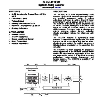
Dac1220 j1z58
December 2019 116More Documents from "Alex Alex" 2s2b68

Ravening Hordes - Lizardmen 8th Ed 2o5e3o
October 2022 0
Dac1220 j1z58
December 2019 116
Aos Warscroll Orruk Brutes En 1gv6n
December 2021 0
Ventajas De La Contabilidad Para Una Empresa 2u313u
June 2021 0
2c82t
May 2020 6